ChipApex | Global Electronic Components Supplier
SEARCH
Search Product
Search Post
— IC芯片 | 连接器 | 传感器 | 被动器件 —
Search productSearch post
— IC芯片 | 连接器 | 传感器 | 被动器件 —
Consult the customer manager about the wholesale price.
consultation hotline:86-132-6715-2157
email:[email protected]
Contact the product manager for consultation. One-stop consultation is available.
Do you want a lower wholesale price? Please send us your inquiry and we will reply immediately.
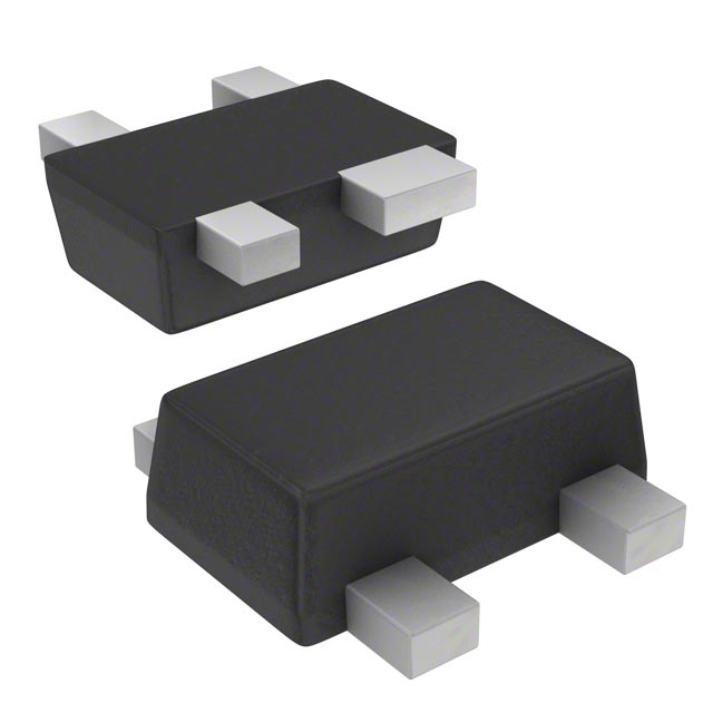
The BFU610F is an NPN silicon microwave transistor designed for high-speed, low-noise applications. It utilizes 40 GHz fT silicon technology and is housed in a plastic SOT343F dual-emitter package with reverse pinning. Key electrical parameters include a collector-base voltage of 16 V, collector-emitter voltage of 5.5 V, and maximum power dissipation of 136 mW at Tsp ≤ 90 °C. The device achieves a noise figure of 1.7 dB and associated gain of 13.5 dB at 5.8 GHz.
Verify the specific ordering suffix to confirm the exact package variant and manufacturing origin. Ensure compliance with ESD handling standards such as ANSI/ESD S20.20 or IEC/ST 61340-5 during storage and assembly. Confirm that the application environment remains within the specified thermal resistance and junction temperature limits to prevent permanent damage.
Select this component for designs requiring low noise performance at microwave frequencies up to 5.8 GHz. Consider the 136 mW power dissipation limit and the requirement for solder point temperature control (Tsp ≤ 90 °C) when designing thermal management solutions. Verify that the operating collector current aligns with the optimal noise figure and gain characteristics provided in the data sheet.
The BFU610F belongs to NXP's portfolio of wideband silicon RF transistors. It is specifically engineered for microwave communication systems where low noise and high gain are critical. The device supports various wireless standards including LTE, Bluetooth, and GPS, making it suitable for modern mobile and IoT connectivity applications.
Consult the official NXP RF Manual or product selection guides for verified substitute part numbers. Do not assume cross-compatibility with other NPN transistors without verifying pinout, voltage ratings, and RF performance metrics against the BFU610F specifications.
The transition frequency is typically 15 GHz under conditions of IC = 4 mA, VCE = 2 V, and f = 2 GHz.
It is available in a plastic surface-mounted flat pack package (SOT343F) with reverse pinning and 4 leads.
The maximum collector-base voltage (VCBO) is 16 V with the emitter open.
 BFU610F,115
The activity of extra discounts on wholesale prices is in full swing…
Please fill in your contact information and we will send you the latest wholesale price list.