 ChipApex | Global Electronic Components Supplier
SEARCH
Search Product
Search Post
— IC芯片 | 连接器 | 传感器 | 被动器件 —
Search productSearch post
— IC芯片 | 连接器 | 传感器 | 被动器件 —
Consult the customer manager about the wholesale price.
consultation hotline:86-132-6715-2157
email:[email protected]
Contact the product manager for consultation. One-stop consultation is available.
Do you want a lower wholesale price? Please send us your inquiry and we will reply immediately.
The Bourns BIDW50N65T is a discrete Insulated Gate Bipolar Transistor (IGBT) utilizing Trench-Gate Field-Stop technology. It features a 650 V collector-emitter voltage rating and a continuous collector current of 100 A at 25 °C case temperature, dropping to 50 A at 100 °C. The device incorporates a built-in fast recovery diode (FRD). Key electrical parameters include a maximum collector-emitter saturation voltage of 2.2 V at 50 A and 25 °C, and a total power dissipation of 416 W. The component operates within a junction temperature range of -55 °C to +150 °C and is housed in a TO-247-3L package.
Verify the specific RoHS compliance status against Directive 2015/863 before finalizing procurement, as regulatory updates may affect material declarations. Confirm that the TO-247-3L package dimensions align with the target PCB footprint and thermal management requirements. Ensure gate drive circuits support the specified ±20 V maximum gate-emitter voltage limits to prevent device damage during operation.
Select this IGBT for high-voltage applications requiring medium-speed switching characteristics. The 650 V rating suits general industrial and consumer power conversion systems. Designers must account for the 10 µs short-circuit withstand time when implementing protection circuits. Verify that the operating junction temperature remains within the -55 °C to +150 °C range under all expected load conditions.
The BIDW50N65T belongs to the BID series of discrete IGBTs manufactured by Bourns. This series combines MOS gate control with bipolar transistor conductivity modulation. The 'W' suffix indicates the TO-247-3L package style, while 'T' denotes the medium-speed optimization variant. This part is distinct from higher or lower voltage ratings within the broader IGBT portfolio.
Consult official Bourns documentation for qualified substitute part numbers. Cross-referencing requires matching the 650 V rating, 50 A continuous current capability, TO-247-3L package, and similar switching energy values to ensure functional compatibility in existing designs.
The device can withstand a short circuit for a maximum duration of 10 µs, measured at VCE = 300 V and VGE = 15 V.
At TC = 25 °C and IC = 50 A, VCE(sat) is typically 1.65 V with a maximum of 2.2 V. At TC = 125 °C under the same conditions, the typical value increases to 1.9 V.
Under standard test conditions (VCE = 400 V, VGE = 15 V, IC = 50 A), the total gate charge (Qg) is typically 123 nC, comprising 31 nC for gate-emitter charge and 48 nC for gate-collector charge.
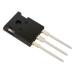 BIDW50N65T
The activity of extra discounts on wholesale prices is in full swing…
Please fill in your contact information and we will send you the latest wholesale price list.




