ChipApex | Global Electronic Components Supplier
SEARCH
Search Product
Search Post
— IC芯片 | 连接器 | 传感器 | 被动器件 —
Search productSearch post
— IC芯片 | 连接器 | 传感器 | 被动器件 —
Consult the customer manager about the wholesale price.
consultation hotline:86-132-6715-2157
email:[email protected]
Contact the product manager for consultation. One-stop consultation is available.
Do you want a lower wholesale price? Please send us your inquiry and we will reply immediately.
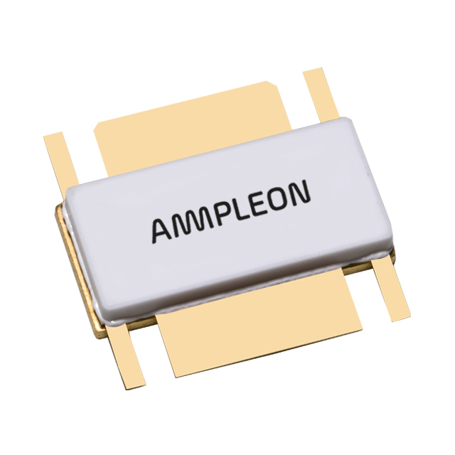
The BLF8G24LS-100V is a 100 W LDMOS power transistor designed for base station applications in the 2300 MHz to 2400 MHz frequency range. It features improved video bandwidth and low memory effects for excellent pre-distortability. The device operates with a drain-source voltage of 28 V and a quiescent current of 900 mA, delivering an average output power of 25 W per carrier in two-carrier W-CDMA configurations. Key electrical parameters include a typical power gain of 19 dB, drain efficiency of 32%, and an adjacent channel power ratio (ACPR) of -29 dBc at 5 MHz spacing. The transistor exhibits high ruggedness, supporting a load mismatch of VSWR = 10:1.
Verify the specific package variant required for the design, as the BLF8G24LS-100V corresponds to the SOT1244B earless flanged ceramic package, while the BLF8G24LS-100GV uses the SOT1244C version. Confirm RoHS compliance status and check the latest product status on the manufacturer's website, as specifications may be updated. Ensure proper ESD precautions are observed during handling due to the sensitivity of the component.
Select this component for broadband operations requiring high efficiency and low thermal resistance. The device is optimized for class-AB operation with test signals such as 3GPP model 1. Designers should account for the specific impedance values provided for source and load matching at 2300 MHz, 2400 MHz, and 2500 MHz to achieve optimal performance metrics like gain and linearity.
This part belongs to the BLF8 series of power LDMOS transistors manufactured by Ampleon USA Inc. The series is characterized by robust construction and suitability for demanding RF power amplifier environments. The BLF8G24LS-100V specifically targets the 2.3 GHz band, offering a balance of power output and linearity for modern communication standards.
The BLF8G24LS-100GV serves as a direct functional equivalent within the same family, differing primarily in the package outline (SOT1244C versus SOT1244B). Both variants share identical electrical characteristics and pinouts, allowing for potential substitution if mechanical footprint constraints permit the alternative package style.
The device typically achieves a video bandwidth of 90 MHz, measured as the IMD third-order intermodulation inflection point in a class-AB test circuit.
Yes, it can withstand a load mismatch corresponding to VSWR = 10:1 through all phases under specified conditions of VDS = 28 V, IDq = 900 mA, and PL = 100 W at 2300 MHz.
The maximum junction temperature (Tj) is 225 °C, although continuous use at maximum temperature will affect reliability.
 BLF8G24LS-100VU
The activity of extra discounts on wholesale prices is in full swing…
Please fill in your contact information and we will send you the latest wholesale price list.