ChipApex | Global Electronic Components Supplier
SEARCH
Search Product
Search Post
— IC芯片 | 连接器 | 传感器 | 被动器件 —
Search productSearch post
— IC芯片 | 连接器 | 传感器 | 被动器件 —
Consult the customer manager about the wholesale price.
consultation hotline:86-132-6715-2157
email:[email protected]
Contact the product manager for consultation. One-stop consultation is available.
Do you want a lower wholesale price? Please send us your inquiry and we will reply immediately.
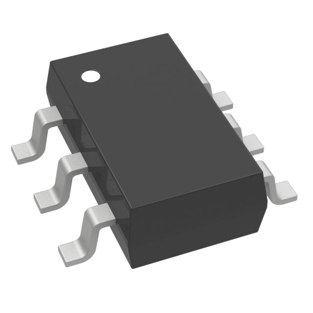
The BSL205NH6327XTSA1 is an OptiMOS®2 dual N-channel enhancement-mode MOSFET in a PG-TSOP6 package. It features a 20 V drain-source voltage and supports up to 2.5 A continuous drain current at 25 °C, with a pulsed capability of 10 A. The device offers a maximum on-state resistance of 85 mΩ at VGS=2.5 V and 50 mΩ at VGS=4.5 V. Key electrical parameters include a gate threshold voltage range of 0.6 V to 1.2 V, total gate charge of 2.1 nC (typical), and power dissipation of 0.5 W. It operates within a temperature range of -55 °C to +150 °C.
Verify the component's authenticity by checking the manufacturer's marking code and ordering suffixes against official Infineon documentation. Ensure that the specific batch meets the required AEC-Q101 qualification standards if used in automotive contexts. Confirm the package type matches the PG-TSOP6 footprint requirements for your PCB layout.
Select this component when a dual N-channel MOSFET with low gate charge and high transconductance is required. Its Super Logic Level feature makes it suitable for systems driven by 2.5 V or 4.5 V logic signals. Consider its thermal resistance and power dissipation limits relative to your ambient operating conditions and PCB copper area availability.
This part belongs to Infineon's OptiMOS®2 family, designed for small-signal and small-power applications. It integrates two independent N-channel transistors into a single compact surface-mount package, optimizing board space while maintaining high performance characteristics typical of the series.
BSL207NH6327XTSA1
The single pulse avalanche energy rating is 10.8 mJ under conditions of ID=2.5 A and RGS=25 Ω.
The integrated reverse diode has a continuous forward current rating of 0.5 A and a typical forward voltage of 0.8 V at 25 °C.
Yes, the BSL205N is Pb-free, RoHS compliant, and halogen-free according to IEC61249-2-21.
 BSL205NH6327XTSA1
The activity of extra discounts on wholesale prices is in full swing…
Please fill in your contact information and we will send you the latest wholesale price list.