ChipApex | Global Electronic Components Supplier
SEARCH
Search Product
Search Post
— IC芯片 | 连接器 | 传感器 | 被动器件 —
Search productSearch post
— IC芯片 | 连接器 | 传感器 | 被动器件 —
Consult the customer manager about the wholesale price.
consultation hotline:86-132-6715-2157
email:[email protected]
Contact the product manager for consultation. One-stop consultation is available.
Do you want a lower wholesale price? Please send us your inquiry and we will reply immediately.
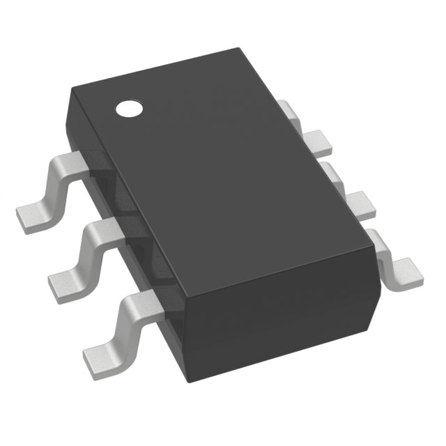
The BSL214NL6327HTSA1 is a dual N-channel small-signal MOSFET from Infineon Technologies, housed in a TSOP-6 surface-mount package. It features a drain-source breakdown voltage of 20 V and a continuous drain current of 2.5 A at 25°C. The device exhibits a maximum on-resistance of 50 mΩ at 4.5 V gate drive. Key electrical parameters include a gate charge of 3.2 nC and an input capacitance of 419 pF. It operates within a junction temperature range of -55°C to +150°C with a power dissipation rating of 500 mW.
Verify the specific suffix HTSA1 against the manufacturer's latest datasheet to confirm tape-and-reel packaging specifications and RoHS compliance status. Ensure the ordering part number matches the exact pinout and thermal characteristics required by the design. Cross-reference with official Infineon distribution channels to validate component authenticity and traceability before integration into production schedules.
Select this component when a dual N-channel topology is required in a TSOP-6 footprint. The 2.5 A current rating and 50 mΩ on-resistance make it suitable for moderate load applications. Consider the 20 V voltage limit and 500 mW power dissipation constraints during thermal management planning. Verify compatibility with 4.5 V logic levels for optimal switching efficiency.
This part belongs to Infineon's BSL series of small-signal MOSFETs, designed for general-purpose switching tasks. The BSL214N variant specifically offers dual channel integration, distinguishing it from single-channel counterparts like the BSS214N. It utilizes silicon technology and is optimized for cost-effective solutions in high-volume consumer electronics manufacturing.
The absolute maximum gate-source voltage is typically ±12 V, consistent with standard small-signal MOSFET specifications in this series.
Public documentation for the BSL214NL6327HTSA1 does not explicitly list AEC-Q100 qualification, unlike some other Infineon variants such as the BSS214NWH6327.
Specific switching timing parameters such as turn-on delay are not explicitly detailed in the provided summary data; refer to the full datasheet for precise dynamic characteristics.
 BSL214NL6327HTSA1
The activity of extra discounts on wholesale prices is in full swing…
Please fill in your contact information and we will send you the latest wholesale price list.