ChipApex | Global Electronic Components Supplier
SEARCH
Search Product
Search Post
— IC芯片 | 连接器 | 传感器 | 被动器件 —
Search productSearch post
— IC芯片 | 连接器 | 传感器 | 被动器件 —
Consult the customer manager about the wholesale price.
consultation hotline:86-132-6715-2157
email:[email protected]
Contact the product manager for consultation. One-stop consultation is available.
Do you want a lower wholesale price? Please send us your inquiry and we will reply immediately.
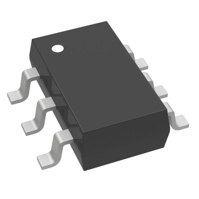
The BSL215CL6327HTSA1 is a dual enhancement-mode MOSFET array from Infineon's OptiMOS series, featuring one P-channel and one N-channel transistor in a TSOP-6 surface-mount package. It supports a drain-source voltage of 20 V with continuous drain currents of 1.5 A for both channels. The device exhibits low on-resistance values of 108 mΩ for the N-channel and 173 mΩ for the P-channel at specified conditions. Operating within a temperature range of -55°C to +150°C, it offers a power dissipation capacity of 500 mW and fast switching characteristics with rise and fall times under 15 ns.
Verify the specific suffix CL against official Infineon documentation to confirm pinout and electrical tolerances, as suffixes often denote tape-and-reel packaging or specific quality grades. Confirm current production status and lifecycle phase directly with the manufacturer or authorized distributors before finalizing design-in decisions.
Select this component when a compact dual MOSFET solution with mixed polarity is required for low-voltage switching applications. The TSOP-6 package suits space-constrained designs, while the AEC-Q101 qualification ensures suitability for automotive environments. Evaluate thermal performance based on the 500 mW power dissipation limit and ambient operating conditions.
This part belongs to Infineon's OptiMOS family, which focuses on optimizing the trade-off between conduction losses and switching speed. The BSL215 series specifically targets cost-sensitive, high-volume applications requiring reliable dual-transistor arrays in small surface-mount packages for power distribution and signal switching tasks.
Consult official cross-reference lists for verified substitutes. Ensure any replacement matches the TSOP-6 footprint, 20 V rating, and dual P/N channel configuration without altering functional parameters.
 BSL215CL6327HTSA1
The activity of extra discounts on wholesale prices is in full swing…
Please fill in your contact information and we will send you the latest wholesale price list.