 ChipApex | Global Electronic Components Supplier
SEARCH
Search Product
Search Post
— IC芯片 | 连接器 | 传感器 | 被动器件 —
Search productSearch post
— IC芯片 | 连接器 | 传感器 | 被动器件 —
Consult the customer manager about the wholesale price.
consultation hotline:86-132-6715-2157
email:[email protected]
Contact the product manager for consultation. One-stop consultation is available.
Do you want a lower wholesale price? Please send us your inquiry and we will reply immediately.
The BSO204P is a dual P-channel OptiMOS-P power transistor in a P-SO 8 package. It features a -20 V drain-source voltage and a maximum on-state resistance of 30 mΩ at VGS = -4.5 V. The device supports a continuous drain current of -7 A at 25°C and handles pulsed currents up to -28 A. Key electrical parameters include an input capacitance of 1513 pF, total gate charge of 35.8 nC, and a reverse diode forward recovery time of 35.9 ns. It operates within a temperature range of -55°C to +150°C.
Verify the specific ordering suffix against the manufacturer's official documentation to confirm exact packaging and tape-and-reel specifications. Ensure the component meets RoHS compliance requirements if applicable to your manufacturing process. Cross-reference the datasheet revision date with your procurement records to guarantee access to the most recent thermal and electrical characteristics.
Select this component for low-voltage applications requiring dual P-channel isolation in a compact surface-mount footprint. Evaluate the 30 mΩ on-resistance against your conduction loss limits at the expected operating current. Confirm that the 2.5 V logic level compatibility matches your controller output voltages for efficient gate driving without additional level shifting circuitry.
This part belongs to Infineon's OptiMOS-P family, designed for general-purpose power switching. It utilizes enhancement mode technology to provide reliable performance in automotive and industrial environments. The P-SO 8 package offers a balance between thermal dissipation capabilities and board space efficiency for dense electronic designs.
Check for direct pin-compatible alternatives within the same OptiMOS-P series that offer lower RDS(on) or higher current ratings. Verify that any substitute maintains the -20 V breakdown voltage and Super Logic Level gate threshold requirements.
The device is rated for 63 mJ of single-pulse avalanche energy under conditions of ID = -7 A, VDD = -10 V, and RGS = 25 Ω.
The integrated reverse diode has a maximum reverse recovery time of 35.9 ns and a dv/dt rating of 6 kV/µs, supporting high-speed commutation.
Yes, the typical gate threshold voltage is 0.9 V, and it is rated as a Super Logic Level device starting at 2.5 V, ensuring reliable turn-on with 3.3 V logic signals.
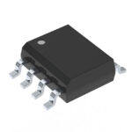 BSO204PNTMA1
The activity of extra discounts on wholesale prices is in full swing…
Please fill in your contact information and we will send you the latest wholesale price list.





