 ChipApex | Global Electronic Components Supplier
SEARCH
Search Product
Search Post
— IC芯片 | 连接器 | 传感器 | 被动器件 —
Search productSearch post
— IC芯片 | 连接器 | 传感器 | 被动器件 —
Consult the customer manager about the wholesale price.
consultation hotline:86-132-6715-2157
email:[email protected]
Contact the product manager for consultation. One-stop consultation is available.
Do you want a lower wholesale price? Please send us your inquiry and we will reply immediately.
The BSO350N03 is an N-channel Power MOSFET from Infineon Technologies, belonging to the OptiMOS2 family. It features a maximum drain-source voltage (VDS) of 30 V and a continuous drain current (ID) of 5 A at 25°C. The device is housed in a DSO-8 surface-mount package. Key electrical characteristics include a typical gate charge (QG) of 6.1 nC at 4.5 V and 12.6 nC at 10 V. The maximum on-resistance (RDS(on)) is specified as 15 mΩ at 10 V gate drive and 18.2 mΩ at 4.5 V gate drive. The component supports a pulsed drain current of 65 A and operates within a junction temperature range of -55°C to 150°C.
Verify component authenticity through authorized Infineon distributors or certified partners. Request original manufacturer documentation and material content sheets to confirm compliance with RoHS and REACH standards. Ensure storage conditions meet semiconductor handling guidelines to prevent moisture sensitivity damage prior to soldering.
Select this component for applications requiring 30 V N-channel switching with moderate current demands. Consider the DSO-8 package for space-constrained PCB layouts. Evaluate thermal management requirements based on the specified RthJA value. Confirm compatibility with logic-level gate drive voltages if operating at lower gate thresholds.
The BSO350N03 is part of Infineon's OptiMOS2 portfolio, designed for high-efficiency power switching. It represents an evolution in power MOSFET technology, offering improved performance over previous generations. The device is engineered for automotive and industrial applications where reliability and efficiency are critical. It complements other OptiMOS variants by providing a balance of voltage rating and current capacity.
The BSO350N03 is marked as obsolete and no longer manufactured. Available substitutes include similar N-channel MOSFETs such as the IRF7313TRPBF. Verify pinout compatibility, electrical parameters, and thermal characteristics when selecting alternative components.
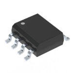 BSO350N03
The activity of extra discounts on wholesale prices is in full swing…
Please fill in your contact information and we will send you the latest wholesale price list.





