 ChipApex | Global Electronic Components Supplier
SEARCH
Search Product
Search Post
— IC芯片 | 连接器 | 传感器 | 被动器件 —
Search productSearch post
— IC芯片 | 连接器 | 传感器 | 被动器件 —
Consult the customer manager about the wholesale price.
consultation hotline:86-132-6715-2157
email:[email protected]
Contact the product manager for consultation. One-stop consultation is available.
Do you want a lower wholesale price? Please send us your inquiry and we will reply immediately.
The BSS138DWK-13 is a dual N-channel enhancement mode MOSFET manufactured by Diodes Incorporated. It features a SOT363 package with two independent channels. Key electrical parameters include a drain-source voltage (BVDSS) of 50V and a gate-source voltage (VGSS) rating of ±20V. The maximum continuous drain current (ID) is 310mA at +25°C, decreasing to 250mA at +70°C. Static on-resistance (RDS(ON)) is specified as 2.6Ω max at VGS=10V, 3.2Ω max at VGS=4.5V, and 5.2Ω max at VGS=2.5V. Total power dissipation is 0.33W on FR-4 PCB with minimum pads, or 0.49W on a 1-inch square copper plate. Operating temperature range spans from -55°C to +150°C.
Verify the specific ordering suffix '-13' corresponds to the 10,000-unit reel packaging format as defined in the manufacturer's ordering information. Confirm that the component meets AEC-Q101 standards if automotive qualification is required, noting that standard versions may differ from qualified variants. Ensure compatibility with J-STD-020 moisture sensitivity level 1 handling procedures during assembly.
Select this component when a dual N-channel topology is required within a minimal footprint. Evaluate the RDS(ON) specifications against the intended gate drive voltage, as resistance varies significantly between 2.5V, 4.5V, and 10V logic levels. Consider the thermal resistance values for the specific PCB copper area available, as power dissipation capabilities depend heavily on the mounting substrate.
This part belongs to the BSS138 family of MOSFETs produced by Diodes Incorporated. While sharing similar voltage ratings and channel types with other family members like the single-channel BSS138, the DWK variant specifically integrates two channels in the SOT363 package. This distinguishes it from single-channel alternatives and provides a solution for space-constrained dual-switching designs.
Direct replacements must match the dual N-channel architecture and SOT363 footprint. Verify that alternative parts meet the 50V BVDSS requirement and provide comparable RDS(ON) characteristics at the target gate drive voltage. Check pinout compatibility, particularly the arrangement of drains, sources, and gates, to ensure interchangeability without circuit redesign.
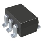 BSS138DWK-13
The activity of extra discounts on wholesale prices is in full swing…
Please fill in your contact information and we will send you the latest wholesale price list.





