 ChipApex | Global Electronic Components Supplier
SEARCH
Search Product
Search Post
— IC芯片 | 连接器 | 传感器 | 被动器件 —
Search productSearch post
— IC芯片 | 连接器 | 传感器 | 被动器件 —
Consult the customer manager about the wholesale price.
consultation hotline:86-132-6715-2157
email:[email protected]
Contact the product manager for consultation. One-stop consultation is available.
Do you want a lower wholesale price? Please send us your inquiry and we will reply immediately.
The BSS138DWQ-7 is a dual N-channel enhancement mode field effect transistor manufactured by Diodes Incorporated. It features a maximum drain-source voltage (VDS) of 50 V and a continuous drain current (ID) of 200 mA at +25°C. The device exhibits a typical static drain-source on-resistance (RDS(ON)) of 1.4 Ω, with a maximum of 3.5 Ω at VGS = 10 V. Gate threshold voltage (VGS(TH)) ranges from 0.5 V to 1.5 V. Total power dissipation is rated at 200 mW, and the junction-to-ambient thermal resistance is 625 °C/W. Operating temperature spans -55°C to +150°C. The component utilizes an SOT363 package and is AEC-Q101 qualified.
Verify that the ordering suffix '-7' corresponds to the 3,000-unit tape and reel carrier format specified in the manufacturer's documentation. Confirm compliance with RoHS 3 directives and ensure the procurement channel is authorized to maintain warranty validity. Cross-reference the date code marking against the official key to validate production year and month accuracy.
Select this component when space-constrained designs require two isolated N-channel switches in a single footprint. Ensure the application gate drive voltage supports the 1.4 Ω to 3.5 Ω RDS(ON) range effectively. Verify that the 200 mA continuous current rating and 200 mW power dissipation limits accommodate the thermal environment without exceeding the 625 °C/W junction-to-ambient resistance constraints.
This part belongs to the BSS138 family of dual N-channel MOSFETs produced by Diodes Incorporated. It shares core electrical characteristics with other variants in the series but differs in packaging and qualification status. The SOT363 form factor distinguishes it from single-channel counterparts like the BSS138W, providing integrated dual-switching capability for complex circuit topologies.
Direct substitutes must match the dual N-channel topology, SOT363 package, and 50V/200mA ratings. Verify equivalent RDS(ON) and VGS(TH) specifications to ensure circuit compatibility. Automotive-grade replacements should also possess AEC-Q101 qualification if the original design intent requires it.
The continuous gate-source voltage (VGSS) is rated at ±20 V.
Yes, the device is AEC-Q101 qualified, PPAP capable, and manufactured in IATF 16949 certified facilities for automotive applications requiring specific change control.
The typical turn-on delay time (tD(ON)) is 20 ns under test conditions of VDD = 30V, ID = 0.2A, and RGEN = 50Ω.
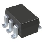 BSS138DWQ-7
The activity of extra discounts on wholesale prices is in full swing…
Please fill in your contact information and we will send you the latest wholesale price list.





