ChipApex | Global Electronic Components Supplier

SEARCH
Search Product
Search Post
— IC芯片 | 连接器 | 传感器 | 被动器件 —
Search productSearch post
— IC芯片 | 连接器 | 传感器 | 被动器件 —
Consult the customer manager about the wholesale price.
consultation hotline:86-132-6715-2157
email:[email protected]
Contact the product manager for consultation. One-stop consultation is available.
Do you want a lower wholesale price? Please send us your inquiry and we will reply immediately.
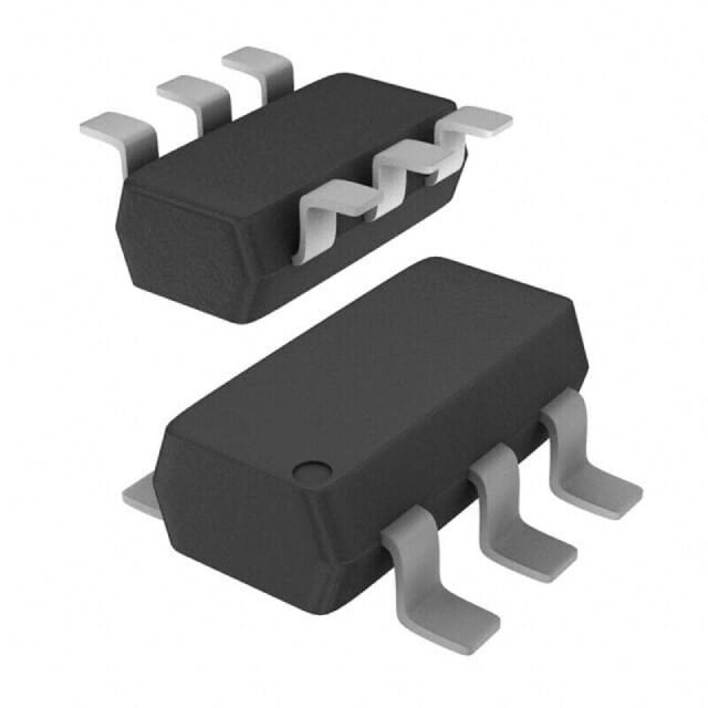
The BSS138KDW is a dual N-channel MOSFET manufactured by Shenzhen Slkormicro Semicon Co., Ltd. in a SOT-363 surface-mount package. It features a drain-source breakdown voltage (VDS) of 50 V and a continuous drain current (ID) of 0.2 A at 25°C. The device has a maximum gate-source voltage (VGS) rating of ±20 V and a junction temperature limit of 150 °C. On-state resistance (RDS(on)) is specified as 5 Ω max at VGS=10V and 6 Ω max at VGS=4.5V, both measured at ID=0.2A. Total gate charge (Qg) is typically 1.7 nC at VGS=10V.
Verify the specific manufacturer part number against official datasheets to confirm electrical parameters and pinout assignments. Ensure the component matches the required SOT-363 package dimensions and thermal characteristics for your design. Cross-reference absolute maximum ratings with your system's operating conditions to prevent device failure.
Select this component when a compact dual N-channel solution is required for low-voltage signal switching or load management. The SOT-363 package offers space efficiency compared to discrete single transistors. Consider the RDS(on) specifications at your intended drive voltage to ensure adequate current handling capabilities within the 0.2 A continuous limit.
This component belongs to the BSS138 series of dual N-channel MOSFETs. It provides two independent N-channel FETs in a single SOT-363 package, designed for applications requiring multiple switching elements in a minimal footprint. The device utilizes standard silicon MOSFET technology optimized for small-signal operations.
Check for compatible dual N-channel MOSFETs in the SOT-363 package with similar VDS and ID ratings. Verify that alternative parts meet the same RDS(on) requirements at your specific gate drive voltages. Ensure pinout compatibility between D1/S1/G1/D2/S2/G2 configurations to maintain circuit functionality without redesign.
The maximum pulse drain current (IDM) is 0.95 A at a case temperature of 25°C.
The typical input capacitance (Ciss) is 18 pF, output capacitance (Coss) is 12 pF, and reverse transfer capacitance (Crss) is 7 pF.
 BSS138KDW

The activity of extra discounts on wholesale prices is in full swing…
Please fill in your contact information and we will send you the latest wholesale price list.