 ChipApex | Global Electronic Components Supplier
SEARCH
Search Product
Search Post
— IC芯片 | 连接器 | 传感器 | 被动器件 —
Search productSearch post
— IC芯片 | 连接器 | 传感器 | 被动器件 —
Consult the customer manager about the wholesale price.
consultation hotline:86-132-6715-2157
email:[email protected]
Contact the product manager for consultation. One-stop consultation is available.
Do you want a lower wholesale price? Please send us your inquiry and we will reply immediately.
The BSS138PS,115 is a dual N-channel enhancement mode Field-Effect Transistor utilizing Trench MOSFET technology within an SOT363 (SC-88) plastic surface-mounted package. It provides two independent channels with a drain-source voltage of 60 V and continuous drain current of 320 mA per transistor at 25 °C. The device features a maximum on-state resistance of 1.6 Ω at VGS = 10 V and gate-source voltage limits of ±20 V. Total power dissipation reaches 420 mW at 25 °C ambient temperature.
Verify the specific ordering suffix
Select this component when space-constrained designs require dual N-channel functionality in a minimal footprint. The SOT363 package supports high-density mounting. Ensure thermal management accounts for the 420 mW total dissipation limit under expected operating conditions.
This part belongs to Nexperia's BSS138 series of small-signal MOSFETs. While single-channel variants like the NX138 exist, the PS variant specifically integrates two channels into one compact package, offering design flexibility for differential or dual-load applications without increasing board area.
Direct functional substitutes include the BSS138BKS, which shares identical electrical characteristics and packaging but may differ in manufacturing origin or specific qualification status. Verify pinout compatibility before substitution.
The device supports a peak drain current of 1.2 A under single-pulse conditions with a duration of 10 μs or less.
Yes, the BSS138PS is qualified in accordance with the AEC-Q101 stress test qualification standard for discrete semiconductors.
The RDS(on) decreases as gate-source voltage increases; it is specified as a maximum of 1.6 Ω at VGS = 10 V and 12 Ω at VGS = 5 V.
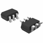 BSS138PS,115
The activity of extra discounts on wholesale prices is in full swing…
Please fill in your contact information and we will send you the latest wholesale price list.





