ChipApex | Global Electronic Components Supplier

SEARCH
Search Product
Search Post
— IC芯片 | 连接器 | 传感器 | 被动器件 —
Search productSearch post
— IC芯片 | 连接器 | 传感器 | 被动器件 —
Consult the customer manager about the wholesale price.
consultation hotline:86-132-6715-2157
email:[email protected]
Contact the product manager for consultation. One-stop consultation is available.
Do you want a lower wholesale price? Please send us your inquiry and we will reply immediately.
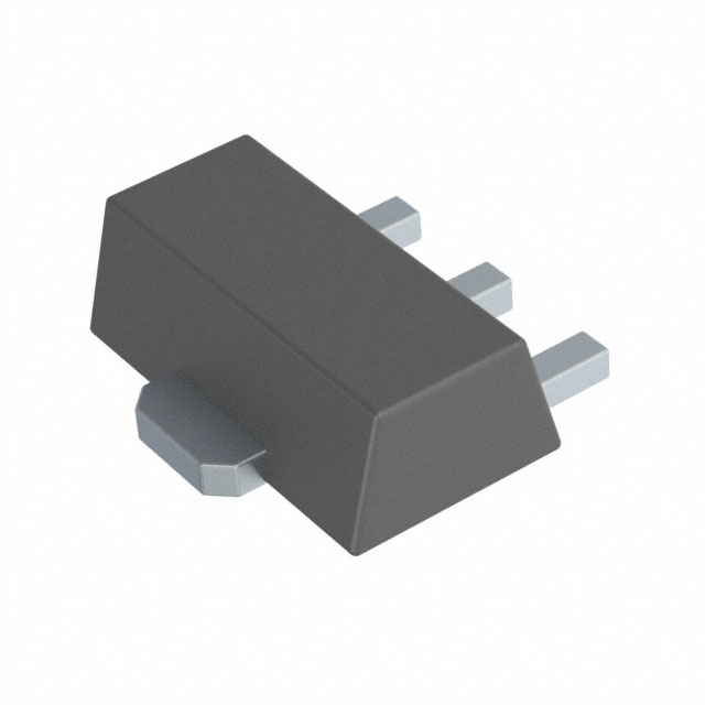
The BSS192,115 is a P-channel vertical Double-Diffused Metal-Oxide-Semiconductor Field-Effect Transistor (D-MOSFET) manufactured by Nexperia. It operates with a drain-source voltage of -240 V and a gate-source voltage range of -20 V to +20 V. The device supports a continuous drain current of -200 mA at 25 °C when the gate-source voltage is -10 V. Its typical on-state resistance is 10 Ω under standard test conditions. The component is housed in a SOT89 surface-mounted package designed for efficient heat transfer.
Verify the specific ordering suffix matches the required packaging configuration before procurement. Confirm that the component version aligns with the latest product data sheet revision history. Ensure the sourcing channel provides authentic Nexperia products to guarantee compliance with specified electrical limits and thermal characteristics.
Select this component for applications requiring high-voltage P-channel switching capabilities within a medium power surface-mount form factor. Evaluate the thermal resistance parameters against the expected junction temperature constraints. Consider the direct logic interface feature to simplify drive circuitry requirements without additional level shifting components.
This device belongs to the Nexperia discrete semiconductor portfolio, specifically categorized as a vertical D-MOS transistor. It utilizes a plastic surface-mounted package with an exposed die pad to facilitate effective thermal dissipation. The component is engineered for robust operation in industrial and consumer electronic environments requiring reliable high-voltage switching.
Consult official Nexperia documentation for verified substitute part numbers. Cross-reference pin configurations and absolute maximum ratings to ensure compatibility. Verify that any alternative component meets the specific voltage and current requirements of the original design.
 BSS192,115

The activity of extra discounts on wholesale prices is in full swing…
Please fill in your contact information and we will send you the latest wholesale price list.