 ChipApex | Global Electronic Components Supplier
SEARCH
Search Product
Search Post
— IC芯片 | 连接器 | 传感器 | 被动器件 —
Search productSearch post
— IC芯片 | 连接器 | 传感器 | 被动器件 —
Consult the customer manager about the wholesale price.
consultation hotline:86-132-6715-2157
email:[email protected]
Contact the product manager for consultation. One-stop consultation is available.
Do you want a lower wholesale price? Please send us your inquiry and we will reply immediately.
The BSS8402DWQ-7 is an automotive-grade complementary pair enhancement mode MOSFET in a SOT363 package. It integrates an N-channel device (Q1) rated at 60V VDS and a P-channel device (Q2) rated at -50V VDS. The Q1 section features a maximum RDS(ON) of 13.5Ω at VGS=10V with a continuous ID of 115mA. The Q2 section offers a maximum RDS(ON) of 10Ω at VGS=-5V with a continuous ID of -130mA. Total power dissipation is 200mW, operating within a junction temperature range of -55°C to +150°C.
Verify the specific ordering suffix to confirm automotive qualification status. The 'Q' suffix indicates AEC-Q101 compliance and IATF 16949 manufacturing origin. Confirm tape and reel quantities match project requirements, as standard and automotive variants share identical electrical specifications but differ in quality control documentation.
Select this component when dual polarity switching is required in a minimal footprint. The SOT363 package supports low input capacitance for fast switching speeds. Ensure gate drive voltages align with the specified threshold ranges for both N-channel and P-channel sections to maintain optimal on-state resistance performance under varying thermal conditions.
This part belongs to Diodes Incorporated's complementary MOSFET family designed for space-constrained designs. It combines two distinct transistors into a single surface-mount package to reduce board area. The Q-series variant specifically targets automotive electronics requiring rigorous change control and reliability standards compared to standard commercial grade parts.
BSS8402DW-7-F: Standard commercial grade equivalent without automotive qualification.
The BSS8402DWQ-7 is AEC-Q101 qualified and manufactured in IATF 16949 certified facilities for automotive use, while the BSS8402DW-7-F is a standard commercial grade part.
The maximum continuous drain current for the P-channel section (Q2) is -130mA at TA = +25°C.
Yes, the device supports a junction temperature range from -55°C to +150°C.
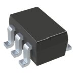 BSS8402DWQ-7
The activity of extra discounts on wholesale prices is in full swing…
Please fill in your contact information and we will send you the latest wholesale price list.





