ChipApex | Global Electronic Components Supplier

SEARCH
Search Product
Search Post
— IC芯片 | 连接器 | 传感器 | 被动器件 —
Search productSearch post
— IC芯片 | 连接器 | 传感器 | 被动器件 —
Consult the customer manager about the wholesale price.
consultation hotline:86-132-6715-2157
email:[email protected]
Contact the product manager for consultation. One-stop consultation is available.
Do you want a lower wholesale price? Please send us your inquiry and we will reply immediately.
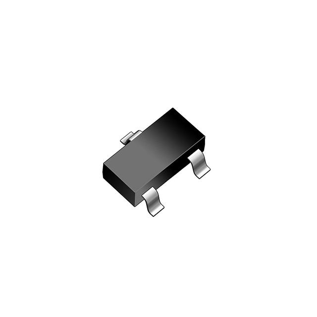
The BSS84AKW is a P-channel enhancement mode MOSFET manufactured by Good-Ark Semiconductor, housed in an SOT-323 surface-mount package. It features a drain-source voltage (VDS) of -60 V and a continuous drain current (ID) of -0.3 A. The device exhibits low on-resistance, with maximum values of 4.7 Ω at VGS = -10 V and 5.7 Ω at VGS = -5 V. Power dissipation is rated at 270 mW, with a junction temperature range up to 150 °C. Gate-source voltage limits are ±20 V, and the component includes ESD protection rated at HBM 2 kV.
Verify the specific manufacturer datasheet for the BSS84AKW when sourcing from Good-Ark Semiconductor or authorized distributors. Confirm that the SOT-323 package dimensions and marking codes match the required design specifications. Ensure compliance with the absolute maximum ratings, particularly regarding the 270 mW power dissipation limit and the 150 °C maximum junction temperature during operation.
Select this component for designs requiring a compact P-channel MOSFET with a 60 V breakdown voltage. The SOT-323 package is suitable for space-constrained PCB layouts. Consider the 4.7 Ω on-resistance at -10 V gate drive when calculating conduction losses. Verify that the -0.3 A continuous current rating meets the load requirements without exceeding thermal limits.
This component belongs to the category of small-signal P-channel MOSFETs designed for general-purpose switching. It serves as a semiconductor solution for controlling power paths in portable electronics. The SOT-323 form factor provides a balance between electrical performance and minimal footprint compared to larger packages.
Cross-reference with other manufacturers' 60 V P-channel MOSFETs in the SOT-323 package. Verify pinout compatibility and ensure that alternative parts meet or exceed the 4.7 Ω RDS(ON) specification at the intended gate drive voltage.
The maximum drain-source voltage (VDS) is -60 V.
Yes, the device features ESD protection rated at HBM 2 kV.
 BSS84AKW

The activity of extra discounts on wholesale prices is in full swing…
Please fill in your contact information and we will send you the latest wholesale price list.