ChipApex | Global Electronic Components Supplier

SEARCH
Search Product
Search Post
— IC芯片 | 连接器 | 传感器 | 被动器件 —
Search productSearch post
— IC芯片 | 连接器 | 传感器 | 被动器件 —
Consult the customer manager about the wholesale price.
consultation hotline:86-132-6715-2157
email:[email protected]
Contact the product manager for consultation. One-stop consultation is available.
Do you want a lower wholesale price? Please send us your inquiry and we will reply immediately.
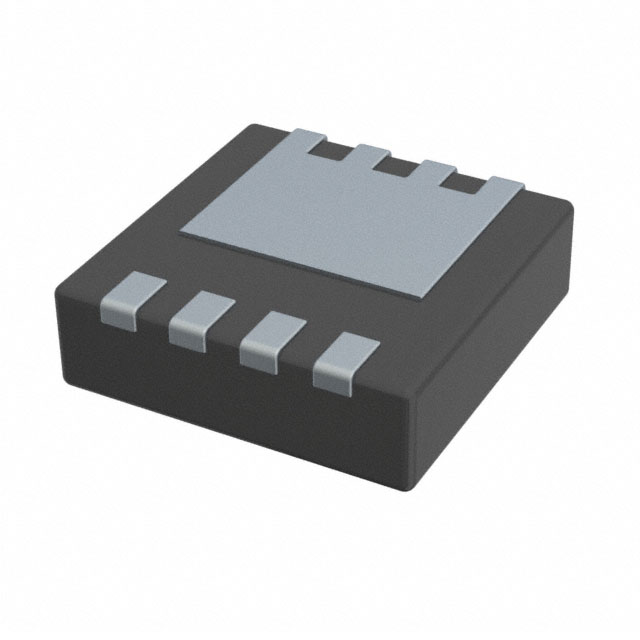
The BSZ180P03NS3EGATMA1 is a P-Channel power MOSFET from Infineon Technologies, part of the OptiMOS P3 family. It features a -30 V drain-source voltage and a continuous drain current of 9 A at Ta or 39.5 A at Tc. The device utilizes a PG-TSDSON-8 surface-mount package with a silicon technology base. Key electrical characteristics include a maximum on-resistance of 8.6 mΩ at 10 V gate drive and a typical gate charge of 43.2 nC. It supports an operating temperature range from -55 °C to +150 °C with a total power dissipation of up to 69 W.
Verify the exact ordering suffix and tape/reel specifications against the official Infineon datasheet before procurement. Confirm that the PG-TSDSON-8 package dimensions match your PCB footprint requirements. Ensure thermal management solutions account for the specified power dissipation limits under your specific operating conditions. Cross-reference the RoHS compliance status with current regulatory standards.
Select this component when a P-Channel MOSFET with low on-resistance and high current capability in a small outline package is required. Compare the 8.6 mΩ Rds(on) and 43.2 nC Qg values against alternative devices to ensure optimal efficiency for your specific switching frequency and load requirements. Consider the thermal resistance characteristics for your enclosure design.
This device belongs to the OptiMOS P3 family of P-channel power MOSFETs by Infineon Technologies. These components are designed to replace older generation technologies, offering improved figure-of-merit metrics. The PG-TSDSON-8 package provides a balance between thermal performance and board space efficiency, suitable for modern consumer and industrial electronics.
Check for direct pin-compatible substitutes within the same OptiMOS P3 series, such as variants with different voltage or current ratings if system margins allow. Verify that any replacement maintains the same PG-TSDSON-8 footprint and thermal characteristics to avoid PCB redesign.
The maximum drain-source voltage (Vds) is -30 V.
The typical gate charge (Qg) is 43.2 nC at a gate-source voltage of 10 V.
It uses the PG-TSDSON-8 surface-mount package.
 BSZ180P03NS3EGATMA1

The activity of extra discounts on wholesale prices is in full swing…
Please fill in your contact information and we will send you the latest wholesale price list.