 ChipApex | Global Electronic Components Supplier

SEARCH
Search Product
Search Post
— IC芯片 | 连接器 | 传感器 | 被动器件 —
Search productSearch post
— IC芯片 | 连接器 | 传感器 | 被动器件 —
Consult the customer manager about the wholesale price.
consultation hotline:86-132-6715-2157
email:[email protected]
Contact the product manager for consultation. One-stop consultation is available.
Do you want a lower wholesale price? Please send us your inquiry and we will reply immediately.
The BUK7E1R8-40E is a standard level N-channel MOSFET utilizing TrenchMOS technology, housed in an I2PAK (SOT226) plastic single-ended package. Designed for high-performance automotive applications and qualified to AEC Q101 standards, it features a drain-source voltage of 40 V and a continuous drain current of 120 A at 25 °C mounting base temperature. The device exhibits a maximum on-state resistance of 1.8 mΩ at 25 °C and supports junction temperatures up to 175 °C.
Verify the specific ordering suffix against the manufacturer's official documentation to ensure correct packaging and tape-and-reel specifications. Confirm that the component meets the required AEC Q101 qualification status for your intended automotive application. Cross-reference the latest datasheet revision to validate thermal characteristics and absolute maximum ratings before finalizing procurement orders.
Select this component when a low on-state resistance is critical for minimizing conduction losses in high-current switching applications. The I2PAK package provides a large mounting base area, facilitating efficient heat dissipation for power densities up to 349 W. Ensure the gate drive circuitry can accommodate the total gate charge requirements while maintaining the specified standard level gate threshold performance across the operating temperature range.
This part belongs to Nexperia's BUK7E series of N-channel TrenchMOS standard level FETs. It is specifically engineered for automotive environments requiring high ruggedness and thermal stability. The I2PAK (SOT226) package distinguishes it from surface-mount variants like LFPAK or TO-263, offering a distinct mechanical footprint optimized for direct mounting to heatsinks via the exposed drain pad.
Direct replacements must match the 40 V rating, 120 A current capacity, and SOT226 package outline. Verify that any substitute maintains AEC Q101 compliance and comparable RDS(on) values. Check pinout compatibility, specifically ensuring the mounting base connection aligns with the drain terminal as defined in the original datasheet.
The maximum non-repetitive drain-source avalanche energy is 1021 mJ under conditions of ID = 120 A, Vsup ≤ 40 V, RGS = 50 Ω, VGS = 10 V, and initial junction temperature of 25 °C.
The device features a true standard level gate with a VGS(th) rating of greater than 1 V at a junction temperature of 175 °C, ensuring reliable turn-on characteristics in thermally demanding environments.
The internal drain inductance (LD) is typically 2.5 nH, measured from the upper edge of the drain mounting base to the center of the die.
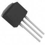 BUK7E1R8-40E,127

The activity of extra discounts on wholesale prices is in full swing…
Please fill in your contact information and we will send you the latest wholesale price list.





