ChipApex | Global Electronic Components Supplier

SEARCH
Search Product
Search Post
— IC芯片 | 连接器 | 传感器 | 被动器件 —
Search productSearch post
— IC芯片 | 连接器 | 传感器 | 被动器件 —
Consult the customer manager about the wholesale price.
consultation hotline:86-132-6715-2157
email:[email protected]
Contact the product manager for consultation. One-stop consultation is available.
Do you want a lower wholesale price? Please send us your inquiry and we will reply immediately.
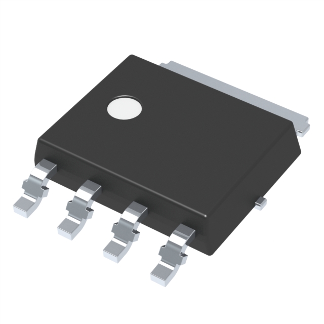
The Nexperia BUK7J1R4-40HX is an automotive qualified N-channel MOSFET utilizing Trench 9 low ohmic superjunction technology within an enhanced LFPAK56E (SOT1023) package. It features a drain-source voltage of 40 V and a maximum continuous drain current of 190 A at a mounting base temperature of 25 °C. The device exhibits a typical drain-source on-state resistance of 1.06 mΩ at VGS = 10 V and ID = 25 A, with a total power dissipation capacity of 395 W. Thermal resistance from junction to mounting base is typically 0.29 K/W.
Verify the specific ordering suffix 'X' corresponds to the reel packaging configuration as defined in the official Nexperia ordering information table. Confirm that the component meets the required AEC-Q101 qualification status for your specific automotive application environment. Ensure the LFPAK56E footprint matches your PCB design guidelines for reflow soldering.
Select this component when high current handling up to 190 A and low conduction losses are critical for 40 V automotive circuits. The tight VGS(th) limits facilitate easy paralleling of multiple devices for higher current sharing. Consider the LFPAK56E package for its superior thermal performance and mechanical robustness compared to traditional QFN packages in high-power density designs.
This part belongs to the BUK7J series of N-channel MOSFETs from Nexperia, designed specifically for automotive applications. It utilizes the SOT1023 (LFPAK56E) plastic surface-mounted package variant. The product is manufactured using silicon technology and is intended for use in high-performance power switching environments requiring high reliability and endurance.
Direct substitutes include other Nexperia BUK7J series parts with similar voltage and current ratings, such as BUK7J1R0-40H, provided the pinout and thermal characteristics match the design requirements. Verify compatibility with existing PCB footprints and thermal management solutions before substitution.
The maximum non-repetitive drain-source avalanche energy is 154 mJ under conditions of ID = 190 A, Vsup ≤ 40 V, RGS = 50 Ω, VGS = 10 V, and initial junction temperature of 25 °C.
The Gull Wing leads provide high board level reliability by absorbing mechanical stress during thermal cycling, which is an advantage over traditional QFN packages that may be more susceptible to stress-induced failures.
Yes, the device features tight VGS(th) limits, which enable easy paralleling of MOSFETs to share current effectively in high-power applications.
 BUK7J1R4-40HX

The activity of extra discounts on wholesale prices is in full swing…
Please fill in your contact information and we will send you the latest wholesale price list.