ChipApex | Global Electronic Components Supplier
SEARCH
Search Product
Search Post
— IC芯片 | 连接器 | 传感器 | 被动器件 —
Search productSearch post
— IC芯片 | 连接器 | 传感器 | 被动器件 —
Consult the customer manager about the wholesale price.
consultation hotline:86-132-6715-2157
email:[email protected]
Contact the product manager for consultation. One-stop consultation is available.
Do you want a lower wholesale price? Please send us your inquiry and we will reply immediately.
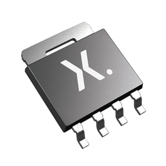
The BUK9Y1R3-40HX is an automotive qualified N-channel MOSFET utilizing Trench 9 low ohmic superjunction technology within a robust LFPAK56 package. It meets AEC-Q101 requirements for high performance and endurance. Key electrical parameters include a drain-source voltage (VDS) of 40 V, a continuous drain current (ID) of 190 A at 25 °C mounting base temperature, and a maximum total power dissipation (Ptot) of 395 W. The device features a typical drain-source on-state resistance (RDSon) of 1.3 mΩ at VGS = 10 V and ID = 25 A. Gate charge (QG(tot)) is typically 99 nC.
Verify the specific ordering suffix matches the required packaging configuration, as variations exist between tape-and-reel and cut-tape formats. Confirm that the component status remains active production rather than obsolete or preliminary. Ensure compliance with REACH and RoHS directives is documented for the specific batch. Check for any recent Product Change Notifications regarding marking codes or package dimensions before finalizing procurement specifications.
Select this component when designing circuits requiring high current handling up to 190 A in a compact surface-mount form factor. The logic-level gate drive capability allows efficient control with standard 4.5 V or 10 V drivers. Consider the LFPAK56 package's thermal advantages for applications where minimizing PCB area is critical but high power dissipation must still be managed effectively through the mounting base.
This device belongs to Nexperia's BUK9Y series of automotive-grade power MOSFETs. It represents the integration of advanced Trench 9 superjunction technology into the LFPAK56 (SOT669) package family. This series is engineered specifically for automotive electronics that demand high reliability, superior thermal performance, and robustness against mechanical stress during operation.
Direct replacements should be sought from the BUK9Y series with equivalent or lower RDSon and compatible VDS ratings. Verify that any substitute maintains the LFPAK56/SOT669 footprint and pinout to ensure mechanical compatibility. Ensure the alternative part also holds AEC-Q101 qualification if automotive reliability is required.
The maximum non-repetitive drain-source avalanche energy (EDS(AL)S) is 154 mJ under conditions of ID = 190 A, Vsup ≤ 40 V, RGS = 50 Ω, VGS = 10 V, and initial junction temperature of 25 °C.
The LFPAK56 package features gull wing leads that enable visual inspection via Automated Optical Inspection (AOI). This eliminates the need for expensive x-ray equipment typically required for traditional QFN packages to verify solder joint quality.
The typical gate-drain charge (QGD) is 11.2 nC, measured at ID = 25 A, VDS = 20 V, and VGS = 4.5 V.
 BUK9Y1R3-40HX
The activity of extra discounts on wholesale prices is in full swing…
Please fill in your contact information and we will send you the latest wholesale price list.