ChipApex | Global Electronic Components Supplier
SEARCH
Search Product
Search Post
— IC芯片 | 连接器 | 传感器 | 被动器件 —
Search productSearch post
— IC芯片 | 连接器 | 传感器 | 被动器件 —
Consult the customer manager about the wholesale price.
consultation hotline:86-132-6715-2157
email:[email protected]
Contact the product manager for consultation. One-stop consultation is available.
Do you want a lower wholesale price? Please send us your inquiry and we will reply immediately.
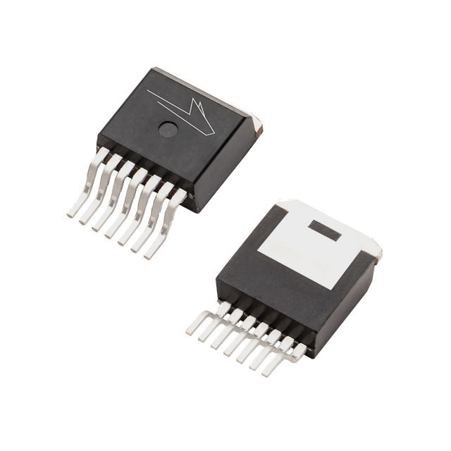
The C3M0040120J1 is a third-generation silicon carbide (SiC) MOSFET from Wolfspeed, housed in a TO-263-7L XL package. It features an N-channel enhancement mode design with a drain-source voltage of 1200 V and a maximum on-resistance of 53.5 mΩ at 150 °C. The device supports a continuous drain current of 64 A and a pulsed current of 100 A. Key electrical parameters include a gate threshold voltage ranging from 1.8 V to 3.6 V, input capacitance of 2900 pF, and total gate charge of 94 nC. Thermal characteristics specify a junction-to-case resistance of 0.46 °C/W, with an operating junction temperature range of -40 °C to +175 °C.
Verify the specific ordering suffix J1 corresponds to the TO-263-7L XL package variant when sourcing. Confirm RoHS compliance status through official Wolfspeed documentation channels prior to integration. Ensure that the selected component matches the exact datasheet revision required for your design specifications. Cross-reference part numbers carefully to distinguish between tape-and-reel and tube packaging options if applicable.
Select this component for designs requiring high efficiency and reduced cooling requirements due to low switching losses. The separate Kelvin source pin facilitates precise gate drive control, minimizing parasitic inductance effects. Consider the thermal resistance and safe operating area curves when designing heat sinks for high-power density applications. Evaluate the gate charge requirements against available driver capabilities to optimize switching frequency performance.
This device belongs to Wolfspeed's C3M series of silicon carbide power MOSFETs. It utilizes advanced third-generation SiC technology to deliver superior performance compared to previous generations. The product line targets high-voltage power conversion applications where efficiency and power density are critical. It represents a continuation of Wolfspeed's leadership in wide-bandgap semiconductor solutions.
Consult official Wolfspeed substitution guides for verified alternatives. Generic cross-references may not match the specific electrical characteristics or package dimensions. Verify compatibility with existing PCB footprints and thermal management strategies before implementing any substitute components.
The separate driver source pin (Kelvin source) isolates the gate drive return path from the high-current power source path. This minimizes ground bounce and reduces gate ringing during switching transitions, improving overall system stability and efficiency.
The maximum transient gate-source voltage is +19 V. For static operation, the recommended turn-on gate voltage is 15 V with a ±5% regulation tolerance. The minimum operational gate-source voltage is -4 V.
The on-resistance increases as the junction temperature rises. At 150 °C, the maximum on-resistance is specified at 53.5 mΩ, compared to a typical value of 40 mΩ at 25 °C under similar test conditions.
 C3M0040120J1-TR
The activity of extra discounts on wholesale prices is in full swing…
Please fill in your contact information and we will send you the latest wholesale price list.