ChipApex | Global Electronic Components Supplier
SEARCH
Search Product
Search Post
— IC芯片 | 连接器 | 传感器 | 被动器件 —
Search productSearch post
— IC芯片 | 连接器 | 传感器 | 被动器件 —
Consult the customer manager about the wholesale price.
consultation hotline:86-132-6715-2157
email:[email protected]
Contact the product manager for consultation. One-stop consultation is available.
Do you want a lower wholesale price? Please send us your inquiry and we will reply immediately.
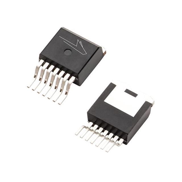
The Wolfspeed C3M0065100J is a Silicon Carbide (SiC) N-Channel Enhancement Mode MOSFET utilizing C3M technology. It features a maximum drain-source voltage of 1000 V and a typical on-state resistance of 65 mΩ at 25°C. The device operates in a TO-263-7 surface-mount package with seven pins, including a dedicated Kelvin source pin for low-inductance gate drive. Key electrical parameters include a continuous drain current of 32 A at 25°C case temperature, a pulsed drain current of 90 A, and a power dissipation rating of 113.5 W. The junction temperature range spans from -55°C to +150°C.
Verify the specific part number against official Wolfspeed documentation to ensure compatibility with design requirements. Confirm that the TO-263-7 package dimensions match the target PCB footprint. Check for RoHS compliance status if required by regional regulations. Ensure sourcing channels provide genuine components to avoid counterfeit risks associated with power semiconductors.
Select this component when designing circuits requiring high-voltage handling up to 1000 V with efficient thermal management. The separate Kelvin source pin is critical for minimizing noise in high-speed switching applications. Consider the thermal resistance characteristics and derating curves for continuous current capabilities at elevated case temperatures. Evaluate the low reverse recovery charge benefits for applications utilizing the internal body diode frequently.
This discrete SiC MOSFET belongs to the C3M product family, representing Wolfspeed's silicon carbide technology. It is designed as an alternative to traditional silicon devices to enable smaller, lighter, and more efficient power conversion systems. The component is intended for industrial and automotive-grade applications where high reliability and performance under harsh conditions are required.
Consult official Wolfspeed documentation for verified substitute part numbers or cross-reference options. Ensure any replacement maintains equivalent voltage ratings, current capabilities, and package dimensions. Verify that thermal and electrical characteristics align with the original design specifications before implementation.
The separate source pin serves as a Kelvin connection for the gate driver. This design separates the high-current source path from the sensitive gate drive return path, minimizing parasitic inductance effects and reducing gate ringing during switching transitions.
The intrinsic body diode is characterized by fast switching speeds and low reverse recovery charge. This feature significantly reduces switching losses when the diode conducts, particularly in hard-switching topologies or synchronous rectification applications.
 C3M0065100J
The activity of extra discounts on wholesale prices is in full swing…
Please fill in your contact information and we will send you the latest wholesale price list.