 ChipApex | Global Electronic Components Supplier
CDC2516DGGR
Search Product
Search Post
— IC芯片 | 连接器 | 传感器 | 被动器件 —
Search productSearch post
— IC芯片 | 连接器 | 传感器 | 被动器件 —
Consult the customer manager about the wholesale price.
consultation hotline:86-132-6715-2157
email:[email protected]
Contact the product manager for consultation. One-stop consultation is available.
Do you want a lower wholesale price? Please send us your inquiry and we will reply immediately.
The CDC2516DGGR is a zero-delay PLL clock driver manufactured by Texas Instruments, designed for high-speed digital systems. It operates within a supply voltage range of 3.0 V to 3.6 V and supports maximum output frequencies up to 400 MHz. The device features a 1:16 multiplication/division factor with differential input and LVPECL/LVCMOS output types. It is housed in a 48-TSSOP package (0.173", 4.40mm width) and functions reliably across an operating temperature range of -40°C to +85°C. This component integrates phase-locked loop circuitry to minimize clock skew.
Verify the specific suffix 'DGGR' corresponds to the TSSOP-48 package and reel packaging configuration before ordering. Confirm that the 3.0 V to 3.6 V supply voltage requirements align with the target system design. Ensure compatibility with LVPECL or LVCMOS load conditions specified in the official datasheet to guarantee signal integrity and proper operation within the industrial temperature range.
Select this component when a zero-delay buffer with integrated PLL functionality is required for frequencies up to 400 MHz. The 1:16 ratio makes it suitable for distributing a single reference clock to sixteen downstream devices. Consider the 48-pin TSSOP footprint for board space constraints. Verify that the differential input requirement matches the source clock generator capabilities and that the LVPECL/LVCMOS outputs meet the impedance matching needs of the destination logic families.
The CDC2516 belongs to Texas Instruments' CDC25xx series of zero-delay PLL clock drivers. These components are engineered to replace traditional discrete clock buffering solutions by integrating frequency multiplication and distribution into a single IC. The DGGR variant specifically denotes the surface-mount TSSOP-48 package form factor, distinguishing it from other pin-compatible or functional equivalents in the broader CDC family.
Publicly confirmed substitute part numbers for the CDC2516DGGR are not available in the provided documentation. Engineers should consult the manufacturer's current selection guide for direct replacements or cross-reference with similar zero-delay PLL drivers such as the CDC2510 or CDC2519, ensuring pinout and electrical specifications match the existing design constraints.
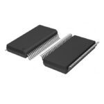 CDC2516DGGR
The activity of extra discounts on wholesale prices is in full swing…
Please fill in your contact information and we will send you the latest wholesale price list.






