ChipApex | Global Electronic Components Supplier
SEARCH
Search Product
Search Post
— IC芯片 | 连接器 | 传感器 | 被动器件 —
Search productSearch post
— IC芯片 | 连接器 | 传感器 | 被动器件 —
Consult the customer manager about the wholesale price.
consultation hotline:86-132-6715-2157
email:[email protected]
Contact the product manager for consultation. One-stop consultation is available.
Do you want a lower wholesale price? Please send us your inquiry and we will reply immediately.
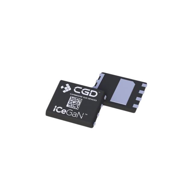
The CGD65B130S2 is a 650 V enhancement-mode GaN HEMT featuring ICeGaN™ gate technology and an integrated current sense function. It offers a typical on-resistance of 130 mΩ and supports a continuous drain current of 12 A at 25 °C case temperature. The device operates with a gate drive voltage range of 9 V to 20 V, compatible with standard Si MOSFET drivers. Packaged in a bottom-side cooled DFN 5x6 mm SMD format, it provides a small PCB footprint while ensuring high thermal performance for high-frequency applications.
Verify the specific ordering suffix against the manufacturer's official documentation to confirm packaging details and tape-and-reel specifications. Ensure that the procurement channel sources components directly from Cambridge GaN Devices or authorized distributors to guarantee authenticity. Confirm that the received parts match the DFN 5x6 mm package dimensions and pinout configuration described in the datasheet before integration into designs.
Select this component for designs requiring high switching frequencies and simplified gate drive interfaces compatible with standard silicon controllers. The integrated current sensing capability makes it suitable for applications where board space is limited and efficiency is critical. Consider the 130 mΩ on-resistance and 12 A current rating when sizing thermal management solutions, as the device relies on the bottom-side thermal pad for heat dissipation.
This device belongs to the ICeGaN™ family of power transistors developed by Cambridge GaN Devices. It utilizes enhancement-mode GaN-on-silicon technology to deliver high breakdown voltage and low on-resistance. The inclusion of an internal Miller clamp and current sense feature distinguishes it from discrete GaN FETs, offering a more integrated solution for power conversion topologies.
Publicly confirmed substitute part numbers are not available in the provided documentation. Designers should consult Cambridge GaN Devices technical support for direct replacements or cross-reference options based on specific electrical and thermal requirements.
The device includes a dedicated current sense output pin (Pin 3) that provides a signal relative to the source. This eliminates the need for an external sense resistor, thereby reducing efficiency losses and simplifying the circuit layout.
The recommended gate drive voltage (VGS in on-state) ranges from 9 V to VDD. The ICeGaN™ gate supply voltage (VDD) is typically recommended at 12 V but can operate up to 20 V.
No. The integrated Miller Clamp within the ICeGaN™ gate technology allows the device to be turned off by setting VGS to 0 V, removing the need for negative gate voltages or external clamping interfaces.
 CGD65B130S2-T13
The activity of extra discounts on wholesale prices is in full swing…
Please fill in your contact information and we will send you the latest wholesale price list.