 ChipApex | Global Electronic Components Supplier
SEARCH
Search Product
Search Post
— IC芯片 | 连接器 | 传感器 | 被动器件 —
Search productSearch post
— IC芯片 | 连接器 | 传感器 | 被动器件 —
Consult the customer manager about the wholesale price.
consultation hotline:86-132-6715-2157
email:[email protected]
Contact the product manager for consultation. One-stop consultation is available.
Do you want a lower wholesale price? Please send us your inquiry and we will reply immediately.
The CP232V-2N4416A is a silicon N-channel JFET bare die designed for VHF amplifier and mixer applications. It features a gate-drain voltage of 35 V, drain-source saturation current (IDSS) ranging from 5.0 to 15 mA, and gate-source cutoff voltage (VGS(OFF)) between 2.5 and 6.0 V. The device exhibits a forward transconductance (gFS) of 4.5 to 7.5 mS and a noise figure of 2.0 dB at 100 MHz. Operating junction temperature spans -65°C to +150°C. Mechanical specifications include a 14 x 14 mils die size, 7.1 mils thickness, and aluminum-silicon top metalization.
Verify the specific packing configuration required for integration, such as unsawn wafer, sawn wafer on plastic ring, or singulated die in waffle packs. Confirm plating requirements by checking for suffixes like TIN/LEAD or PBFREE if applicable. Ensure design validation covers all field use cases and extreme conditions as per manufacturer disclaimers.
Select this component when designing sensitive VHF circuits requiring low noise and high breakdown voltage. Consider the bare die form factor for custom packaging solutions. Evaluate thermal management capabilities given the wide operating temperature range up to +150°C. Verify compatibility with existing substrate materials for bonding pad metallization.
This part represents a discrete semiconductor die manufactured by Central Semiconductor Corp. It corresponds to the functional characteristics of the 2N4416A family but is supplied without an external package. It serves as a foundational component for hybrid microwave integrated circuits or specialized RF modules where standard packages are unsuitable.
Direct replacements may include other N-channel JFET dies with similar BVGSS and IDSS ranges. Verify pinout compatibility if transitioning to packaged equivalents like the TO-72 or SOT-23 versions of the 2N4416A. Ensure mechanical dimensions and metallization layers match the target assembly process.
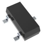 CP232V-2N4416A-CT
The activity of extra discounts on wholesale prices is in full swing…
Please fill in your contact information and we will send you the latest wholesale price list.





