 ChipApex | Global Electronic Components Supplier
SEARCH
Search Product
Search Post
— IC芯片 | 连接器 | 传感器 | 被动器件 —
Search productSearch post
— IC芯片 | 连接器 | 传感器 | 被动器件 —
Consult the customer manager about the wholesale price.
consultation hotline:86-132-6715-2157
email:[email protected]
Contact the product manager for consultation. One-stop consultation is available.
Do you want a lower wholesale price? Please send us your inquiry and we will reply immediately.
The CSD25303W1015 is a P-channel NexFET power MOSFET designed for ultra-low on-resistance and gate charge within a compact CSP package. It features a –20 V drain-to-source voltage rating and supports a continuous drain current of –3 A at 25°C case temperature. The device utilizes a 1 × 1.5 mm DSBGA-6 wafer level package with a maximum height of 0.62 mm. Key electrical parameters include a typical RDS(on) of 46 mΩ at VGS = –4.5 V, a total gate charge (Qg) of 3.3 nC at –4.5 V, and a threshold voltage (VGS(th)) ranging from –0.4 V to –1 V. Thermal resistance (RqJA) is specified at 198 °C/W for minimum copper area and 112 °C/W for a 1 in² copper area.
Verify the specific ordering suffix and packaging configuration against the manufacturer's latest documentation before procurement. Confirm that the component status aligns with project requirements, as availability classifications may change. Ensure design inputs match the absolute maximum ratings provided in the official datasheet to prevent device failure during operation.
Select this component when minimizing board space and reducing switching losses are primary design constraints. The low Qg and Qgd values make it suitable for high-frequency switching applications. Evaluate thermal performance based on the actual PCB copper area available, as thermal resistance varies significantly between minimum and 1 in² copper configurations.
This device belongs to the NexFET family of power MOSFETs from Texas Instruments. It is engineered to deliver superior performance metrics in a minimal outline package compared to traditional surface-mount technologies. The wafer level package construction contributes to its low thermal impedance and small physical dimensions.
Check for updated product lifecycle statuses such as LIFEBUY or OBSOLETE before finalizing designs. Verify pinout compatibility and electrical parameter overlaps if substituting with other P-channel MOSFETs in the same voltage class.
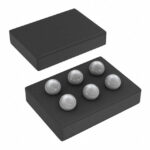 CSD25303W1015
The activity of extra discounts on wholesale prices is in full swing…
Please fill in your contact information and we will send you the latest wholesale price list.





