 ChipApex | Global Electronic Components Supplier
SEARCH
Search Product
Search Post
— IC芯片 | 连接器 | 传感器 | 被动器件 —
Search productSearch post
— IC芯片 | 连接器 | 传感器 | 被动器件 —
Consult the customer manager about the wholesale price.
consultation hotline:86-132-6715-2157
email:[email protected]
Contact the product manager for consultation. One-stop consultation is available.
Do you want a lower wholesale price? Please send us your inquiry and we will reply immediately.
The CSD75301W1015 is a dual P-channel NexFET Power MOSFET from Texas Instruments, housed in a compact 6-DSBGA (1mm × 1.5mm) surface-mount package with a maximum height of 0.62mm. It features a drain-to-source voltage rating of -20V and a continuous drain current of -1.2A at 25°C. The device achieves an ultra-low on-resistance of 80mΩ at VGS = -4.5V and a total gate charge of 1.5nC at -4.5V. Designed for high efficiency, it operates within a junction temperature range of -55°C to 150°C and offers a power dissipation capacity of 0.8W.
Verify the component status before procurement as this specific part number may be discontinued or subject to production changes. Confirm that the required tape and reel packaging aligns with manufacturing equipment specifications. Ensure the final assembly process accommodates the small DSBGA outline and low-profile solder ball dimensions to maintain thermal and mechanical integrity.
Select this component when minimizing board area is critical due to its 1mm by 1.5mm package size. It is appropriate for low-voltage applications requiring efficient switching, given its low gate charge characteristics. Evaluate the thermal resistance requirements carefully, as the small footprint limits heat dissipation capabilities compared to larger packages.
This device belongs to the NexFET family of power MOSFETs, which are engineered to provide the lowest possible on-resistance and gate charge within minimal outlines. The CSD75301W1015 specifically targets portable electronics and battery-powered devices where space and energy efficiency are primary design constraints.
Check for direct cross-references or updated revisions within the manufacturer's portfolio. Verify pinout compatibility and electrical parameters if substituting with other dual P-channel MOSFETs in similar packages.
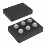 CSD75301W1015
The activity of extra discounts on wholesale prices is in full swing…
Please fill in your contact information and we will send you the latest wholesale price list.





