ChipApex | Global Electronic Components Supplier
SEARCH
Search Product
Search Post
— IC芯片 | 连接器 | 传感器 | 被动器件 —
Search productSearch post
— IC芯片 | 连接器 | 传感器 | 被动器件 —
Consult the customer manager about the wholesale price.
consultation hotline:86-132-6715-2157
email:[email protected]
Contact the product manager for consultation. One-stop consultation is available.
Do you want a lower wholesale price? Please send us your inquiry and we will reply immediately.
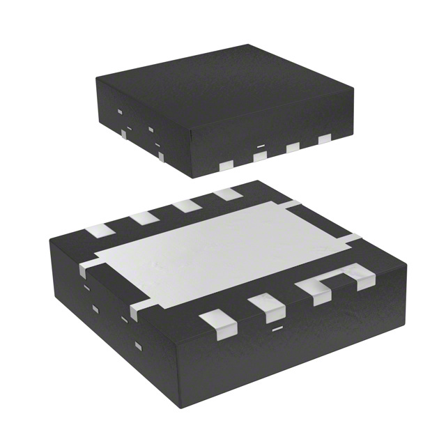
The CSD87333Q3D is a dual N-channel NexFET Power Block from Texas Instruments, housed in an 8-pin VSON package. It features a drain-source breakdown voltage of 30 V and a continuous drain current of 15 A. The device exhibits a typical on-resistance of 14.3 mΩ at room temperature. Gate-source voltage limits are specified between -8 V and +8 V, with a threshold voltage of 1.2 V. Total gate charge is 3.5 nC. Switching characteristics include a rise time of 3.9 ns and a fall time of 2.2 ns. The component operates within a junction temperature range of -55°C to +150°C and supports a power dissipation of 1.5 W.
Verify the specific ordering suffix against the manufacturer's official datasheet to confirm pinout compatibility and electrical specifications. Ensure that the procurement documentation matches the exact part number variant required for the design. Cross-reference the RoHS and REACH compliance status with the latest regulatory filings before finalizing orders.
Select this component when a compact solution for 30-V synchronous rectification is required. The low gate charge facilitates driving by standard logic-level controllers without external buffers. Evaluate the thermal resistance parameters relative to the target PCB copper area to ensure the junction temperature remains within safe operating limits under maximum load conditions.
This device belongs to the CSD8733x series of NexFET Power Blocks designed for space-constrained power management applications. It integrates two N-channel MOSFETs into a single monolithic structure, reducing footprint compared to discrete solutions. The series targets high-frequency DC-DC conversion where efficiency and size are critical constraints.
Direct replacements must match the 30-V rating, 8-pin VSON package, and dual N-channel configuration. Verify that substitute components offer comparable Rds(on) and gate charge values to maintain switching performance. Check for identical pin assignments to avoid PCB redesign requirements during implementation.
 CSD87333Q3D
The activity of extra discounts on wholesale prices is in full swing…
Please fill in your contact information and we will send you the latest wholesale price list.