ChipApex | Global Electronic Components Supplier
SEARCH
Search Product
Search Post
— IC芯片 | 连接器 | 传感器 | 被动器件 —
Search productSearch post
— IC芯片 | 连接器 | 传感器 | 被动器件 —
Consult the customer manager about the wholesale price.
consultation hotline:86-132-6715-2157
email:[email protected]
Contact the product manager for consultation. One-stop consultation is available.
Do you want a lower wholesale price? Please send us your inquiry and we will reply immediately.
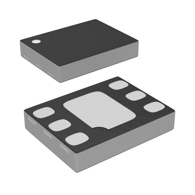
The CTLDM7120-M621H TR is a surface-mount N-channel enhancement-mode silicon MOSFET manufactured by Central Semiconductor Corp. It features a TLM621H package with an exposed thermal pad internally connected to the drain pins. The device supports a drain-source voltage of 20 V and a continuous drain current of 1.0 A at 25°C. Key electrical parameters include a maximum gate-source voltage of 8.0 V, a threshold voltage range of 0.5 V to 1.2 V, and a total gate charge of 2.4 nC. The on-resistance varies from 0.075 Ω to 0.25 Ω depending on the gate drive voltage and drain current conditions.
Verify End-of-Life status before design finalization. Confirm availability through authorized distributors or stock-only channels as production has ceased. Request updated datasheets and replacement part recommendations directly from Central Semiconductor engineering support to ensure component continuity in existing designs.
Select this component for applications requiring a compact N-channel MOSFET with logic-level gate drive capability. Ensure the operating junction temperature remains within the -65°C to +150°C range. Verify that the PCB layout accommodates the TLM621H package dimensions and utilizes thermal vias to connect the exposed pad to the ground plane for optimal heat dissipation.
This device belongs to the Central Semiconductor enhancement-mode N-channel MOSFET family utilizing DMOS process technology. It is designed specifically for high-speed switching applications where low threshold voltage and fast response times are critical requirements for efficient power management in small form factor electronics.
No direct replacement part numbers are listed in official documentation. Consult Central Semiconductor engineering for alternate sourcing options.
The exposed pad (Pin P) is internally connected to Pins 2, 3, 4, and 5, which correspond to the Drain terminals.
The maximum pulsed drain current is 4.0 A with a pulse width of 10 microseconds.
 CTLDM7120-M621H TR
The activity of extra discounts on wholesale prices is in full swing…
Please fill in your contact information and we will send you the latest wholesale price list.