 ChipApex | Global Electronic Components Supplier

SEARCH
Search Product
Search Post
— IC芯片 | 连接器 | 传感器 | 被动器件 —
Search productSearch post
— IC芯片 | 连接器 | 传感器 | 被动器件 —
Consult the customer manager about the wholesale price.
consultation hotline:86-132-6715-2157
email:[email protected]
Contact the product manager for consultation. One-stop consultation is available.
Do you want a lower wholesale price? Please send us your inquiry and we will reply immediately.
CY23FS04ZXI-3T is listed in the Clock Generators, PLLs, Frequency Synthesizers range at ChipApex. The manufacturer field lists Infineon Technologies. Its product description is IC FANOUT DIST 16TSSOP. Review the specifications below when checking this part for your BOM.
The CY23FS04ZXI-3T is a Failsafe zero delay buffer manufactured by Infineon Technologies (formerly Cypress Semiconductor). It features an internal digitally controlled crystal oscillator (DCXO) for continuous glitch-free operation. The device provides four phase-aligned outputs with zero input-output propagation delay and low jitter of 35 ps max RMS. It supports reference inputs from 4.17 MHz to 166.7 MHz and delivers outputs up to 166.7 MHz. Operating voltages include 2.5 V or 3.3 V for VDD and 3.3 V for the core supply VDDC. It is housed in a 16-pin TSSOP package and operates within an industrial temperature range of -40 °C to +85 °C.
Verify the ordering suffix 'T' indicates tape and reel packaging configuration. Confirm the 'I' suffix corresponds to the industrial temperature grade ranging from -40 °C to +85 °C. Ensure the specific part number matches the required voltage and package specifications before procurement.
Select this component when zero delay buffering and failover capability are critical. Verify that the external crystal frequency is an integer factor of the desired reference clock frequency. Check that the load capacitance requirements align with the specified 15 pF maximum for high-frequency outputs.
This device belongs to the Failsafe family of zero delay buffers designed for robust clock management. It integrates a DCXO to serve as a redundant clock source, synchronizing with external references when available. The architecture simplifies system design by eliminating complex switching circuitry typically required for redundancy.
Direct replacements must support the same 16-pin TSSOP package and industrial temperature range. Verify compatibility with 2.5 V/3.3 V output supplies and 3.3 V core supply. Ensure the substitute offers comparable jitter performance and DCXO functionality for failover applications.
The internal DCXO maintains the last known frequency and phase information, providing continuous glitch-free operation while the FAIL#/SAFE pin indicates the failure status.
The crystal frequency connected to the DCXO must be an integer factor of the reference clock frequency, determined by the S select lines.
Yes, the PLL and DCXO bypass mode allows operation, though normal synchronization requires a valid reference input within the capture range.
Explore related parts through Clock/Timing, Integrated Circuits (ICs), all product categories, ChipApex homepage.
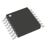 CY23FS04ZXI-3T

The activity of extra discounts on wholesale prices is in full swing…
Please fill in your contact information and we will send you the latest wholesale price list.





