ChipApex | Global Electronic Components Supplier
SEARCH
Search Product
Search Post
— IC芯片 | 连接器 | 传感器 | 被动器件 —
Search productSearch post
— IC芯片 | 连接器 | 传感器 | 被动器件 —
Consult the customer manager about the wholesale price.
consultation hotline:86-132-6715-2157
email:[email protected]
Contact the product manager for consultation. One-stop consultation is available.
Do you want a lower wholesale price? Please send us your inquiry and we will reply immediately.
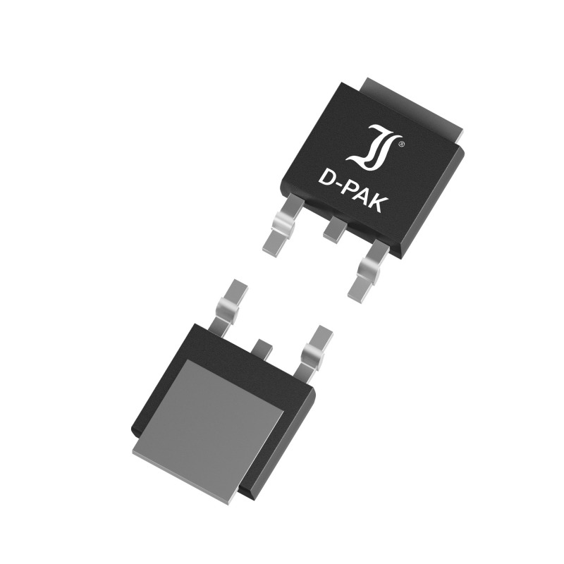
The DI022P06D1 is a P-Channel Power MOSFET manufactured by Diotec Semiconductor, utilizing advanced trench technology. It features a drain-source voltage of -60 V and a continuous drain current of -22 A at 25°C case temperature. The device exhibits a maximum on-state resistance of 45 mΩ at VGS = -10 V and ID = -10 A. With a power dissipation rating of 43 W and an avalanche energy capability of 30 mJ, it supports fast switching times including turn-on delay of 11 ns and fall time of 4 ns. The component operates within a junction temperature range of -55°C to +150°C.
Verify the specific suffix when ordering. The standard version is commercial grade. Suffix -Q indicates AEC-Q101 compliance, while -AQ denotes qualification in progress. Confirm package type TO-252AA (D-PACK) and tape-and-reel quantity of 2500 units per 13-inch reel. Ensure thermal management aligns with the specified RthJC of 2.9 K/W.
Select this component for applications requiring high current handling in a compact D-PACK footprint. The low on-state resistance minimizes conduction losses. Consider the -Q variant if automotive reliability standards are required. Evaluate thermal performance based on the 35 K/W junction-to-ambient resistance for PCB mounting scenarios.
This part belongs to Diotec's P-Channel MOSFET lineup designed for general-purpose power switching. It shares the TO-252AA mechanical outline common across the series but differs in electrical ratings compared to N-Channel variants like the DI020N06D1. The marking code '06P450' identifies the specific device on the casing.
Public confirmed substitute part numbers are not available in the provided documentation.
The DI022P06D1 is rated for 30 mJ of single pulse avalanche energy under test conditions of ID = -24.5 A, VG = -10 V, L = 0.1 mH, and RG = 25 Ω.
At VGS = -10 V and ID = -10 A, the maximum RDS(on) is 45 mΩ. At a lower gate drive of VGS = -4.5 V and ID = -8 A, the maximum RDS(on) increases to 60 mΩ.
 DI022P06D1
The activity of extra discounts on wholesale prices is in full swing…
Please fill in your contact information and we will send you the latest wholesale price list.