ChipApex | Global Electronic Components Supplier
SEARCH
Search Product
Search Post
— IC芯片 | 连接器 | 传感器 | 被动器件 —
Search productSearch post
— IC芯片 | 连接器 | 传感器 | 被动器件 —
Consult the customer manager about the wholesale price.
consultation hotline:86-132-6715-2157
email:[email protected]
Contact the product manager for consultation. One-stop consultation is available.
Do you want a lower wholesale price? Please send us your inquiry and we will reply immediately.
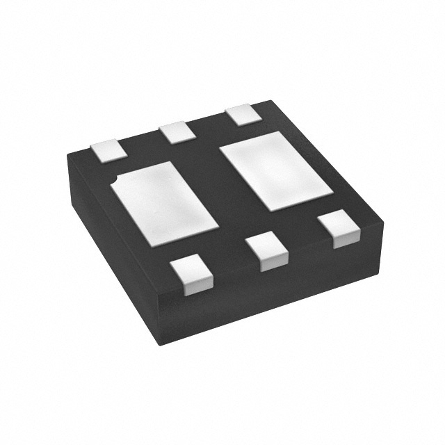
The DMC1029UFDB-7 is a complementary pair enhancement mode MOSFET manufactured by Diodes Incorporated. It integrates one N-channel and one P-channel device in a U-DFN2020-6 package with a maximum height of 0.6mm. The N-channel transistor provides a drain-source voltage (BVDSS) of 12V, while the P-channel offers -12V. Maximum continuous drain currents are 5.6A for the N-channel and -3.8A for the P-channel at +25°C. On-resistance values are 29mΩ max for the N-channel at VGS=4.5V and 61mΩ max for the P-channel at VGS=-4.5V. Total power dissipation is rated at 1.4W steady state.
Verify the specific ordering suffix against official documentation before procurement. The '-7' suffix indicates a standard tape and reel packaging quantity of 3000 units. Confirm that the required component version matches the exact datasheet revision and manufacturing site specifications to ensure compliance with project requirements.
Select this component when a compact dual MOSFET solution is required for low-voltage power paths. The U-DFN2020-6 package is suitable for space-constrained designs. Ensure gate drive voltages align with the specified thresholds for optimal RDS(ON) performance. Verify thermal management capabilities based on the 1.4W steady-state power dissipation rating.
This part belongs to the DMC1029 series of complementary enhancement mode MOSFETs from Diodes Incorporated. It shares functional characteristics with other devices in the family but differs in package type and electrical ratings. The UFDB suffix denotes the specific U-DFN2020-6 physical form factor used in this configuration.
Direct substitutes include the DMC1029UFDB-13, which utilizes the same internal die and package but comes in a 10000-unit tape and reel format. Other compatible options within the DMC series should be evaluated based on matching voltage, current, and package dimensions.
The maximum operating and storage temperature range for the junction is -55°C to +150°C.
The N-channel RDS(ON) decreases as gate voltage increases, ranging from a maximum of 65mΩ at VGS=1.5V to 29mΩ at VGS=4.5V. The P-channel RDS(ON) similarly improves from 210mΩ at VGS=-1.5V to 61mΩ at VGS=-4.5V.
For automotive applications requiring specific change control, AEC-Q qualification, or IATF 16949 manufacturing, customers must contact Diodes Incorporated directly, as standard parts may not meet these specific criteria.
 DMC1029UFDB-7
The activity of extra discounts on wholesale prices is in full swing…
Please fill in your contact information and we will send you the latest wholesale price list.