ChipApex | Global Electronic Components Supplier
SEARCH
Search Product
Search Post
— IC芯片 | 连接器 | 传感器 | 被动器件 —
Search productSearch post
— IC芯片 | 连接器 | 传感器 | 被动器件 —
Consult the customer manager about the wholesale price.
consultation hotline:86-132-6715-2157
email:[email protected]
Contact the product manager for consultation. One-stop consultation is available.
Do you want a lower wholesale price? Please send us your inquiry and we will reply immediately.
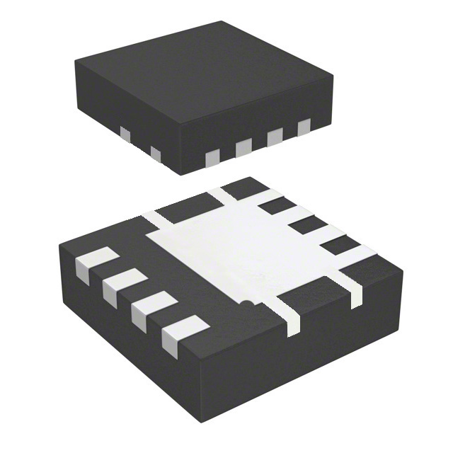
The DMC3016LDV-7 is a complementary pair enhancement mode MOSFET manufactured by Diodes Incorporated. It integrates an N-channel and a P-channel device within a single PowerDI3333-8 (Type UXC) package. The N-channel transistor provides a drain-source breakdown voltage of 30 V, with a maximum on-resistance of 12 mΩ at VGS = 10 V and a continuous drain current of 21 A at TC = +25°C. The P-channel counterpart features a -30 V breakdown voltage, a maximum on-resistance of 25 mΩ at VGS = -10 V, and a continuous drain current of -15 A under the same thermal conditions. Both channels operate within a junction temperature range of -55°C to +150°C.
Verify the specific ordering suffix '-7' against official documentation to confirm the 2,000-unit tape and reel packaging format. Ensure that the component meets the required environmental standards, specifically RoHS compliance and the absence of intentionally added lead, halogens, and antimony as defined by the manufacturer's green product guidelines.
Select this component when a dual-channel solution is required for space-constrained designs utilizing the PowerDI3333-8 footprint. Evaluate the thermal performance based on the application's PCB copper area, as the datasheet specifies distinct power dissipation ratings depending on whether the board uses minimum pad layouts or extensive thermal biasing to the bottom layer.
This part belongs to the DMC3016 series of advanced complementary MOSFETs from Diodes Incorporated. The series is engineered to minimize on-state resistance while maintaining superior switching performance. The 'LDV' designation indicates the specific electrical characteristics and package type, distinguishing it from other variants in the family such as those with different pin configurations or thermal profiles.
DMC3016LSD-13
The maximum pulsed drain current for the N-channel device is 70 A, measured with a 380μs pulse duration and a duty cycle of 1%.
The gate threshold voltage exhibits a negative temperature coefficient, decreasing as the ambient temperature increases from -55°C to +150°C.
The typical total gate charge is 9.5 nC when tested at VGS = 4.5 V, and 21 nC when tested at VGS = 10 V.
 DMC3016LDV-7
The activity of extra discounts on wholesale prices is in full swing…
Please fill in your contact information and we will send you the latest wholesale price list.