ChipApex | Global Electronic Components Supplier
SEARCH
Search Product
Search Post
— IC芯片 | 连接器 | 传感器 | 被动器件 —
Search productSearch post
— IC芯片 | 连接器 | 传感器 | 被动器件 —
Consult the customer manager about the wholesale price.
consultation hotline:86-132-6715-2157
email:[email protected]
Contact the product manager for consultation. One-stop consultation is available.
Do you want a lower wholesale price? Please send us your inquiry and we will reply immediately.
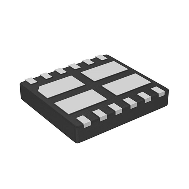
The DMHC10H170SFJ-13 is a complementary enhancement mode MOSFET H-bridge array manufactured by Diodes Incorporated. It integrates two N-channel and two P-channel transistors within a single V-DFN5045-12 package. The N-channel devices feature a drain-source voltage (BVDSS) of 100V, with maximum on-resistance (RDS(ON)) values of 160mΩ at VGS=10V and 200mΩ at VGS=4.5V. Continuous drain current ratings are 2.9A at 25°C and 2.3A at 70°C. The P-channel devices provide -100V BVDSS, with RDS(ON) maximums of 250mΩ at VGS=-10V and 300mΩ at VGS=-4.5V. Total power dissipation is rated at 2.1W.
Verify the specific ordering suffix '-13' corresponds to the 3,000-unit tape and reel packaging configuration. Confirm that the component meets the required automotive qualification standards if intended for AEC-Q100/101/104/200 applications, as standard production may differ from qualified facility output.
Select this component when a compact, complementary H-bridge solution is required for 100V systems. Ensure gate drive voltages align with the specified thresholds for optimal RDS(ON) performance. Verify thermal management capabilities against the 60°C/W junction-to-ambient resistance rating for the target operating environment.
This device belongs to the DMHC10 series of complementary MOSFET arrays from Diodes Incorporated. It utilizes the V-DFN5045-12 surface-mount package, designed for automated assembly. The product represents a generation focused on balancing low on-state resistance with fast switching characteristics for modern power electronics.
Direct pin-compatible replacements must be sourced from official manufacturer cross-reference lists. Verify that any substitute maintains the same 100V rating, H-bridge topology, and V-DFN5045-12 footprint without altering electrical parameters significantly.
The N-channel devices support a continuous drain current of 2.9A at an ambient temperature of +25°C, which decreases to 2.3A at +70°C.
The gate threshold voltage exhibits negative temperature coefficient behavior, decreasing as the junction temperature increases, as illustrated in the typical characteristics graphs.
The body diode reverse recovery charge (QRR) is typically 35.2 nC when tested at IS = 12.8A and dI/dt = 100A/μs.
 DMHC10H170SFJ-13
The activity of extra discounts on wholesale prices is in full swing…
Please fill in your contact information and we will send you the latest wholesale price list.