ChipApex | Global Electronic Components Supplier

SEARCH
Search Product
Search Post
— IC芯片 | 连接器 | 传感器 | 被动器件 —
Search productSearch post
— IC芯片 | 连接器 | 传感器 | 被动器件 —
Consult the customer manager about the wholesale price.
consultation hotline:86-132-6715-2157
email:[email protected]
Contact the product manager for consultation. One-stop consultation is available.
Do you want a lower wholesale price? Please send us your inquiry and we will reply immediately.
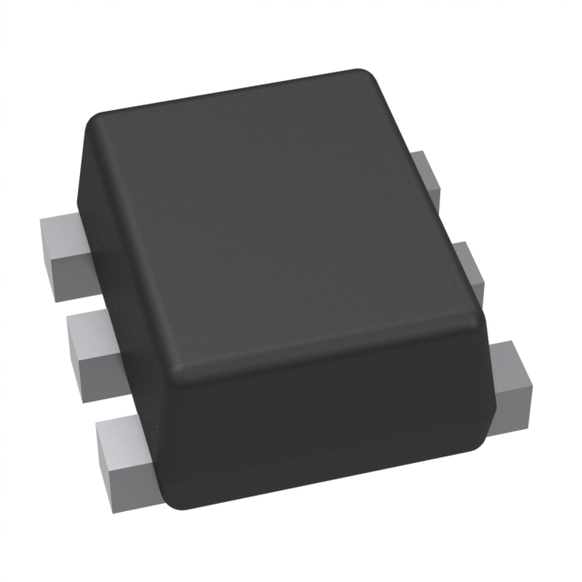
The DMN2991UDJ-7 is a dual N-channel enhancement mode MOSFET manufactured by Diodes Incorporated. It features a maximum drain-source voltage (BVDSS) of 20V and a gate-source voltage (VGSS) rating of ±8V. The device offers low on-state resistance, with RDS(ON) values ranging from 0.48Ω to 2.4Ω depending on the gate drive voltage and current conditions. Continuous drain current capabilities vary between 330mA and 520mA at +25°C. Packaged in an ultra-small SOT963 surface mount case measuring 1mm x 1mm with a maximum height of 0.45mm, it supports a total power dissipation of 0.4W and operates within a temperature range of -55°C to +150°C.
Verify the specific ordering suffix when purchasing. The DMN2991UDJ-7A variant includes a Pin 1 indicator marking, whereas the standard DMN2991UDJ-7 does not. Both variants share identical electrical characteristics and are supplied in 10K tape and reel packaging. Confirm compliance requirements such as RoHS and halogen-free status directly with the manufacturer or authorized distributors before finalizing procurement orders.
Select this component for applications requiring compact dual N-channel MOSFET solutions with low on-resistance. Ensure the gate drive voltage meets the minimum requirements for the desired RDS(ON) level, as performance varies significantly between 1.5V and 4.5V gate thresholds. Consider the thermal constraints of the SOT963 package, which has a junction-to-ambient thermal resistance of 312°C/W, for high-efficiency power management designs.
This part belongs to the DMN2991 series of dual N-channel enhancement mode MOSFETs produced by Diodes Incorporated. The series is designed to minimize on-state resistance while maintaining superior switching performance. The DMN2991UDJ-7 specifically utilizes the SOT963 package, offering a small footprint suitable for space-constrained portable and general-purpose electronic applications.
The DMN2991UDJ-7A serves as a direct functional replacement for the DMN2991UDJ-7, differing only in the presence of a Pin 1 indicator marking. No other electrical or mechanical differences exist between these two part numbers according to official documentation.
The maximum continuous gate-source voltage (VGSS) rating is ±8V.
RDS(ON) decreases as gate voltage increases. At VGS = 4.5V, RDS(ON) is typically 0.48Ω, while at VGS = 1.5V, it rises to approximately 0.97Ω typical.
For automotive applications requiring specific change control, AEC-Q100/101/200 qualification, PPAP capability, and manufacturing in IATF 16949 certified facilities, customers must contact Diodes Incorporated directly.
 DMN2991UDJ-7

The activity of extra discounts on wholesale prices is in full swing…
Please fill in your contact information and we will send you the latest wholesale price list.