ChipApex | Global Electronic Components Supplier

SEARCH
Search Product
Search Post
— IC芯片 | 连接器 | 传感器 | 被动器件 —
Search productSearch post
— IC芯片 | 连接器 | 传感器 | 被动器件 —
Consult the customer manager about the wholesale price.
consultation hotline:86-132-6715-2157
email:[email protected]
Contact the product manager for consultation. One-stop consultation is available.
Do you want a lower wholesale price? Please send us your inquiry and we will reply immediately.
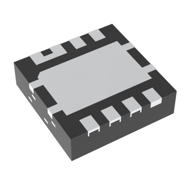
The DMN3012LFG-13 is a dual N-channel enhancement mode MOSFET manufactured by Diodes Incorporated. It features a PowerDI3333-8 (Type D) surface-mount package. The device provides a drain-source voltage rating of 30V and continuous drain currents up to 20A at case temperatures of +25°C. Q1 exhibits a maximum on-resistance of 12mΩ, while Q2 achieves 6mΩ, both measured at VGS = 5V and ID = 15A. Gate-source voltage limits are ±10V. Thermal characteristics include a junction-to-case resistance of 9.5°C/W and a total power dissipation of 2.2W at TC = +25°C. Operating and storage temperature ranges span from -55°C to +150°C.
Verify component authenticity upon receipt, as the datasheet explicitly marks this part as not recommended for new design. Confirm that the received units match the specified PowerDI3333-8 (Type D) package dimensions and marking codes. Ensure sourcing channels provide valid traceability documentation to mitigate risks associated with obsolete or discontinued inventory.
Engineers should prioritize the successor model DMN3012LDG for any new hardware development cycles due to the explicit obsolescence notice in the official documentation. Evaluate thermal constraints carefully, as the 2.2W power dissipation limit requires adequate PCB copper area for heat spreading. Verify gate drive voltages do not exceed the ±10V absolute maximum rating to prevent gate oxide breakdown.
This component belongs to the DMN3012 series of synchronous N-channel enhancement mode MOSFETs produced by Diodes Incorporated. It utilizes the PowerDI3333-8 (Type D) plastic molded package designed for efficient thermal transfer. The specific suffix '-13' indicates a tape and reel packaging quantity of 3000 units per reel, distinct from the '-7' variant which contains 1000 units.
The official datasheet recommends using DMN3012LDG as the direct replacement for this component. Designers must verify pin compatibility and electrical parameter alignment before substituting the legacy DMN3012LFG-13 with the suggested DMN3012LDG in existing circuits.
The absolute maximum rating for the gate-source voltage (VGSS) is ±10V.
Q1 has a maximum RDS(ON) of 12mΩ, whereas Q2 offers a lower maximum RDS(ON) of 6mΩ under identical test conditions.
No, the datasheet explicitly states 'NOT RECOMMENDED FOR NEW DESIGN' and directs users to use the DMN3012LDG instead.
 DMN3012LFG-13

The activity of extra discounts on wholesale prices is in full swing…
Please fill in your contact information and we will send you the latest wholesale price list.