 ChipApex | Global Electronic Components Supplier
SEARCH
Search Product
Search Post
— IC芯片 | 连接器 | 传感器 | 被动器件 —
Search productSearch post
— IC芯片 | 连接器 | 传感器 | 被动器件 —
Consult the customer manager about the wholesale price.
consultation hotline:86-132-6715-2157
email:[email protected]
Contact the product manager for consultation. One-stop consultation is available.
Do you want a lower wholesale price? Please send us your inquiry and we will reply immediately.
The ALD1105SBL is a monolithic dual N-channel and dual P-channel complementary matched MOSFET pair housed in a 14-pin SOIC plastic package. It features a low threshold voltage of 0.7V, low input capacitance of 3pF, and an offset voltage of 10mV. The device operates within a temperature range of 0°C to +70°C with a maximum drain-source voltage of 10V and power dissipation of 500mW.
Verify the specific suffix 'SBL' corresponds to the 14-pin SOIC plastic package variant when ordering. Confirm that the operating temperature range meets the application requirements of 0°C to +70°C. Ensure static control procedures are followed due to ESD sensitivity. Check for lead-free (RoHS) compliance as indicated by the 'L' suffix.
Select the ALD1105SBL for analog applications requiring high input impedance and low leakage currents. Consider the 10V drain-source voltage limit and 500mW power dissipation rating. Evaluate the need for thermal tracking between matched pairs. Compare against similar devices like the ALD1103 if higher current capabilities are required.
The ALD1105 is part of Advanced Linear Devices' ACMOS silicon gate CMOS process family. It combines an ALD1116 N-channel pair and an ALD1117 P-channel pair into a single package. This integration allows for compact designs in precision signal switching and amplifying applications.
The ALD1103 is a related device with higher current capabilities. Verify pin compatibility and electrical parameter differences before substitution. Consult the manufacturer for alternative packages or high-temperature versions if needed.
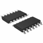 ALD1105SBL
The activity of extra discounts on wholesale prices is in full swing…
Please fill in your contact information and we will send you the latest wholesale price list.





