ChipApex | Global Electronic Components Supplier

SEARCH
Search Product
Search Post
— IC芯片 | 连接器 | 传感器 | 被动器件 —
Search productSearch post
— IC芯片 | 连接器 | 传感器 | 被动器件 —
Consult the customer manager about the wholesale price.
consultation hotline:86-132-6715-2157
email:[email protected]
Contact the product manager for consultation. One-stop consultation is available.
Do you want a lower wholesale price? Please send us your inquiry and we will reply immediately.
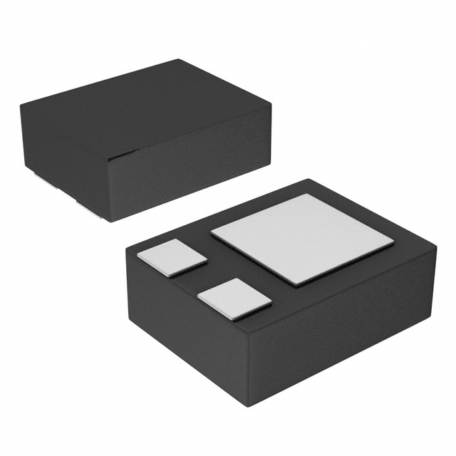
The DMN31D5UFA-7B is an N-channel enhancement mode MOSFET manufactured by Diodes Incorporated. It features a maximum drain-source voltage (V_DSS) of 30 V and a gate-source voltage (V_GSS) rating of ±12 V. The device operates within a temperature range of -55 °C to +150 °C. At V_GS = 4.5 V, the maximum on-resistance (R_DS(ON)) is 1.5 Ω with a continuous drain current (I_D) of 0.4 A. Lower gate voltages result in higher resistance and reduced current capacity: at V_GS = 2.5 V, R_DS(ON) is 2.0 Ω (I_D = 0.35 A); at V_GS = 1.8 V, it is 3.0 Ω (I_D = 0.3 A); and at V_GS = 1.5 V, it reaches 4.5 Ω (I_D = 0.23 A).
Verify the specific ordering suffix '-7B' against official manufacturer documentation to confirm packaging details, as datasheets may list variations such as tape and reel quantities. Ensure compliance requirements match project needs, specifically checking for RoHS 2/3 directives and Halogen/Antimony-free status. Confirm the X2-DFN0806-3 package dimensions and recommended pad layout are compatible with the target PCB design before finalizing procurement.
Select this component when space constraints require a footprint significantly smaller than traditional SOT23 packages. It is suitable for applications requiring low on-resistance at varying gate drive voltages, including 1.5 V to 4.5 V ranges. Consider the thermal characteristics and maximum power dissipation limits when designing for high ambient temperatures or continuous operation conditions.
This part belongs to the DMN31D5UFA series of N-channel enhancement mode MOSFETs from Diodes Incorporated. It is packaged in an X2-DFN0806-3 format, providing a compact solution for surface-mount assembly. The device is designed to offer a balance between low conduction losses and fast switching speeds, making it appropriate for modern portable and battery-powered electronics.
Public confirmed substitute part numbers are not available in the provided source material.
The maximum gate threshold voltage (V_GS(TH)) is 1.0 V, measured at V_DS = V_GS and I_D = 250 μA.
The on-resistance increases as the junction temperature rises. Graphical data indicates variation across the operating range from -55 °C to +150 °C, with higher temperatures resulting in increased R_DS(ON).
Yes, the forward voltage (V_SD) of the body diode is specified, ranging from a typical 0.6 V to a maximum of 1.0 V at a source current of 10 mA.
 DMN31D5UFA-7B

The activity of extra discounts on wholesale prices is in full swing…
Please fill in your contact information and we will send you the latest wholesale price list.