 ChipApex | Global Electronic Components Supplier

SEARCH
Search Product
Search Post
— IC芯片 | 连接器 | 传感器 | 被动器件 —
Search productSearch post
— IC芯片 | 连接器 | 传感器 | 被动器件 —
Consult the customer manager about the wholesale price.
consultation hotline:86-132-6715-2157
email:[email protected]
Contact the product manager for consultation. One-stop consultation is available.
Do you want a lower wholesale price? Please send us your inquiry and we will reply immediately.
The DMN5L06DWK-7 is a dual N-channel enhancement mode MOSFET manufactured by Diodes Incorporated. It features a maximum drain-source voltage (Vdss) of 50 V and a continuous drain current (Id) of 305 mA at 25°C. The device has a gate-source threshold voltage (Vgs(th)) of 1.0 V max at 250 µA. Static drain-source on-resistance (Rds(on)) is specified as 2.0 Ω at Vgs = 5.0 V, Id = 50 mA, and 3.0 Ω at Vgs = 1.8 V, Id = 50 mA. Total power dissipation (Pd) is 250 mW at 25°C ambient temperature. The component is housed in an SOT363 surface mount package.
Verify the specific ordering suffix matches the required packaging quantity. Confirm compliance with RoHS and halogen-free requirements if environmental regulations apply. Check for the 'Not Recommended for New Design' notice and evaluate alternative components for new projects. Ensure the supplier provides valid traceability documentation for the manufacturing date code.
Select this component when a compact dual N-channel solution is required for low-voltage switching applications. Consider the 50 V breakdown voltage and 305 mA current limits against circuit demands. Evaluate the thermal resistance of 500 °C/W for heat dissipation constraints. Verify that the logic-level gate threshold supports the available drive voltage levels in the design.
This part belongs to the DMN series of dual N-channel MOSFETs from Diodes Incorporated. It utilizes the SOT363 case outline, which houses two independent channels in a six-terminal surface mount footprint. The device is designed for general-purpose switching and load control tasks where space efficiency is critical.
The datasheet explicitly recommends using DMN61D9UDW as a replacement or alternative for new designs due to the 'Not Recommended for New Design' status of this component.
No, the datasheet marks this component as 'Not Recommended for New Design' and suggests using DMN61D9UDW instead.
The maximum operating junction temperature (TJ) is +150 °C.
Yes, the device is ESD protected up to 2kV.
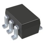 DMN5L06DWK-7-01

The activity of extra discounts on wholesale prices is in full swing…
Please fill in your contact information and we will send you the latest wholesale price list.





