 ChipApex | Global Electronic Components Supplier

SEARCH
Search Product
Search Post
— IC芯片 | 连接器 | 传感器 | 被动器件 —
Search productSearch post
— IC芯片 | 连接器 | 传感器 | 被动器件 —
Consult the customer manager about the wholesale price.
consultation hotline:86-132-6715-2157
email:[email protected]
Contact the product manager for consultation. One-stop consultation is available.
Do you want a lower wholesale price? Please send us your inquiry and we will reply immediately.
The DMN601DWK-7 is a dual N-channel enhancement mode MOSFET in an SOT363 package. It features a drain-source voltage of 60V and a continuous drain current of 305mA at 25°C. The maximum static drain-source on-resistance is 3Ω at VGS=5V and 0.05A, or 2Ω at VGS=10V and 0.5A. Total power dissipation is 200mW with a thermal resistance of 625°C/W. Operating temperature ranges from -65°C to +150°C.
Verify the component against Diodes Incorporated datasheet DS30656 Rev. 11-2. Confirm the marking code K7K YM matches the specific batch. Ensure the device meets JEDEC standards for high reliability if required for automotive applications. Check that the packaging corresponds to the standard tape and reel format specified for this part number.
Select this component for applications requiring a compact dual N-channel solution with moderate voltage ratings. The SOT363 package is suitable for surface-mount assembly where board space is limited. Consider the 3Ω on-resistance at 5V drive when designing logic interfaces. Evaluate the 200mW power dissipation limit under expected operating conditions.
This device belongs to the DMN601 series of dual N-channel enhancement mode field effect transistors manufactured by Diodes Incorporated. It utilizes silicon technology housed in a molded plastic SOT363 package. The product is lead-free, fully RoHS compliant, and halogen-free.
An automotive-compliant version is available as DMN601DWKQ. Verify pinout compatibility and electrical parameters before substituting with other dual N-channel MOSFETs in the SOT363 package.
The maximum pulsed drain current is 800mA, provided the pulse width is less than or equal to 10µs and the duty cycle is less than or equal to 1%.
Yes, the internal schematic indicates the presence of gate protection diodes for each channel.
The typical total gate charge (Qg) is 304pC, measured at VGS=4.5V, VDS=10V, and ID=250mA.
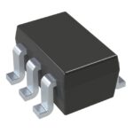 DMN601DWK-7

The activity of extra discounts on wholesale prices is in full swing…
Please fill in your contact information and we will send you the latest wholesale price list.





