 ChipApex | Global Electronic Components Supplier
SEARCH
Search Product
Search Post
— IC芯片 | 连接器 | 传感器 | 被动器件 —
Search productSearch post
— IC芯片 | 连接器 | 传感器 | 被动器件 —
Consult the customer manager about the wholesale price.
consultation hotline:86-132-6715-2157
email:[email protected]
Contact the product manager for consultation. One-stop consultation is available.
Do you want a lower wholesale price? Please send us your inquiry and we will reply immediately.
The DMP3007LSS-13 is a P-channel enhancement mode MOSFET manufactured by Diodes Incorporated. It features a drain-source voltage (V_DSS) of -30 V and an SO-8 surface-mount package. The device exhibits low on-resistance, specified as a maximum of 7 mΩ at V_GS = -10 V and 10 mΩ at V_GS = -4.5 V. Continuous drain current ratings are -17 A at +25°C for short pulses and -14 A in steady-state conditions. Key electrical parameters include a total gate charge of 64.2 nC at V_GS = -10 V, input capacitance of 2826 pF, and a junction temperature range from -55°C to +150°C.
Verify the specific ordering suffix '-13' corresponds to the 2,500-unit tape and reel packaging configuration. Confirm that the component meets the required UL flammability classification rating of 94V-0 and moisture sensitivity level 3 per J-STD-020 standards for your assembly process. Ensure compatibility with matte tin annealed over copper leadframe terminal finishes.
Select this component when a low R_DS(ON) value is critical for minimizing conduction losses in P-channel switching applications. Evaluate the thermal resistance characteristics against your board layout requirements, specifically noting the difference between single-sided FR-4 and multi-layer substrate performance. Consider the gate threshold voltage variations across the operating temperature range to ensure reliable turn-on under varying load conditions.
This part belongs to the DMP series of P-channel enhancement mode MOSFETs from Diodes Incorporated. It utilizes an SO-8 case constructed from molded plastic green molding compound. The internal schematic indicates a built-in gate protection diode. The marking code 'P3007LS' identifies the product type, followed by date code markings for traceability.
No public confirmed substitute part numbers are documented in the provided source material.
The maximum continuous drain current is -14 A at a steady state ambient temperature of +25°C, and -11.5 A at +70°C. For short duration pulses (t<10s), it can handle up to -17 A at +25°C.
The static drain-source on-resistance is maximized at 7 mΩ when V_GS is -10 V. At a lower gate drive of -4.5 V, the maximum R_DS(ON) increases to 10 mΩ.
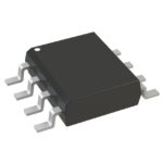 DMP3007LSS-13
The activity of extra discounts on wholesale prices is in full swing…
Please fill in your contact information and we will send you the latest wholesale price list.





