ChipApex | Global Electronic Components Supplier
SEARCH
Search Product
Search Post
— IC芯片 | 连接器 | 传感器 | 被动器件 —
Search productSearch post
— IC芯片 | 连接器 | 传感器 | 被动器件 —
Consult the customer manager about the wholesale price.
consultation hotline:86-132-6715-2157
email:[email protected]
Contact the product manager for consultation. One-stop consultation is available.
Do you want a lower wholesale price? Please send us your inquiry and we will reply immediately.
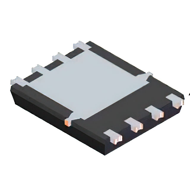
The DMP4006SPSW-13 is a 40V P-channel enhancement mode MOSFET manufactured by Diodes Incorporated. It utilizes the PowerDI5060-8 package and offers a maximum drain-source on-resistance of 5.2mΩ at VGS = -10V and 7.9mΩ at VGS = -6V. The device supports a continuous drain current of -115A at TC = +25°C and features a gate threshold voltage range of -2.0V to -3.0V. It includes wettable flank terminals for improved optical inspection and is qualified to JEDEC standards.
Verify the specific ordering suffix matches the required packaging configuration, as indicated in the manufacturer's documentation. Confirm that the component meets RoHS compliance requirements and halogen-free specifications if mandated by your design constraints. Ensure the selected part number aligns with the intended thermal and electrical operating conditions defined in the datasheet.
Select this component when a low-profile surface-mount solution is required for high-current applications. The PowerDI5060-8 package provides robust thermal dissipation capabilities suitable for demanding environments. Consider the specific gate drive voltage levels, as the on-resistance varies significantly between -6V and -10V operation points.
This component belongs to the DMP series of P-channel MOSFETs from Diodes Incorporated. It represents a newer generation of devices engineered to balance low conduction losses with fast switching speeds. The product line targets modern electronic systems requiring compact footprints and high reliability.
For automotive applications requiring specific change control, refer to the related automotive grade parts with the Q-suffix. These variants are qualified to AEC-Q standards and manufactured in IATF 16949 certified facilities.
The wettable flank design allows solder to flow around the side of the leads, enabling better visual inspection of solder joints using automated optical inspection systems.
The static drain-source on-resistance is lower at higher gate voltages; it is specified as 5.2mΩ max at VGS = -10V and 7.9mΩ max at VGS = -6V.
 DMP4006SPSW-13
The activity of extra discounts on wholesale prices is in full swing…
Please fill in your contact information and we will send you the latest wholesale price list.