ChipApex | Global Electronic Components Supplier
SEARCH
Search Product
Search Post
— IC芯片 | 连接器 | 传感器 | 被动器件 —
Search productSearch post
— IC芯片 | 连接器 | 传感器 | 被动器件 —
Consult the customer manager about the wholesale price.
consultation hotline:86-132-6715-2157
email:[email protected]
Contact the product manager for consultation. One-stop consultation is available.
Do you want a lower wholesale price? Please send us your inquiry and we will reply immediately.
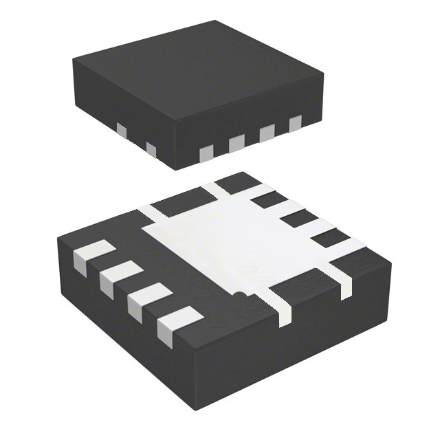
The DMP6023LFG-7 is a P-channel enhancement mode MOSFET from Diodes Incorporated, housed in a POWERDI3333-8 package. It features a -60V drain-source voltage rating and a maximum continuous drain current of -7.7A at +25°C. The device offers a low on-state resistance of 25mΩ at VGS = -10V and 33mΩ at VGS = -4.5V. Key electrical parameters include a gate threshold voltage ranging from -1V to -3V, an input capacitance of 2569pF, and a total gate charge of 53.1nC at VGS = -10V. It operates within a junction temperature range of -55°C to +150°C.
Verify the specific ordering suffix when purchasing. The datasheet lists DMP6023LFG-7 as packaged in 2,000-unit tape and reel quantities. Confirm that the received component matches the exact part number and packaging specification required for your assembly process to ensure compatibility with automated placement equipment.
Select this component for designs requiring a compact P-channel MOSFET with low on-resistance. Ensure the application voltage does not exceed the -60V drain-source breakdown limit. Consider the thermal characteristics and package size when designing PCB layouts, particularly if operating near the maximum rated currents or temperatures.
This component belongs to the DMP series of P-channel enhancement mode MOSFETs manufactured by Diodes Incorporated. It is designed for high-density power management solutions where space constraints are critical. The POWERDI3333-8 package provides a balance between thermal performance and footprint reduction compared to traditional surface mount packages.
Direct replacements must match the -60V rating, P-channel type, and POWERDI3333-8 package. Verify that any substitute maintains equivalent RDS(ON) values and gate charge specifications to ensure similar switching behavior and thermal performance in the target circuit.
The maximum pulsed drain current (IDM) is -55A, specified with a 10µs pulse duration and a 1% duty cycle.
Yes, the device is qualified to AEC-Q101 standards for high reliability, making it suitable for automotive environments.
The body diode reverse recovery time (trr) is typically 20ns, measured at an forward current of -5A and a di/dt of 100A/μs.
 DMP6023LFG-7
The activity of extra discounts on wholesale prices is in full swing…
Please fill in your contact information and we will send you the latest wholesale price list.