 ChipApex | Global Electronic Components Supplier
SEARCH
Search Product
Search Post
— IC芯片 | 连接器 | 传感器 | 被动器件 —
Search productSearch post
— IC芯片 | 连接器 | 传感器 | 被动器件 —
Consult the customer manager about the wholesale price.
consultation hotline:86-132-6715-2157
email:[email protected]
Contact the product manager for consultation. One-stop consultation is available.
Do you want a lower wholesale price? Please send us your inquiry and we will reply immediately.
The DMP6111SVT-7 is a P-channel enhancement mode MOSFET manufactured by Diodes Incorporated. It features a drain-source breakdown voltage of -60V and a maximum continuous drain current of -2.7A at +25°C. The device offers a typical on-resistance of 87mΩ at VGS = -10V and 112mΩ at VGS = -4.5V. Total gate charge is 23.2nC at VGS = -10V. Operating temperature ranges from -55°C to +150°C.
Verify the specific ordering suffix '-7' corresponds to the 3,000-unit tape and reel packaging configuration. Confirm that the component meets the required environmental standards, specifically RoHS compliance and the absence of intentionally added lead, halogens, and antimony as defined by the manufacturer's green product definitions.
Select this component when a single P-channel MOSFET in a TSOT26 package is required for compact designs. Ensure the application operates within the specified -60V drain-source voltage limit and requires a continuous current capability of up to -2.7A at ambient temperatures of +25°C. Consider thermal derating for operation above +25°C or in confined spaces.
This part belongs to the DMP6111SVT series of P-channel enhancement mode MOSFETs. It is distinct from the dual-channel variant DMP6110SVT-13. An automotive-compliant version, DMP6111SVTQ, is available under a separate datasheet for applications requiring specific automotive qualification standards beyond standard industrial reliability.
DMP6110SVT-13 is a related dual-channel variant but differs in channel count and current rating.
The standard DMP6111SVT-7 is qualified to JEDEC standards for high reliability. For specific automotive requirements, an automotive-compliant part (DMP6111SVTQ) is available under a separate datasheet.
The maximum operating and storage temperature range for the DMP6111SVT-7 extends up to +150°C.
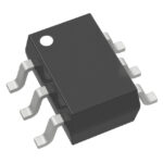 DMP6111SVT-7
The activity of extra discounts on wholesale prices is in full swing…
Please fill in your contact information and we will send you the latest wholesale price list.





