 ChipApex | Global Electronic Components Supplier

SEARCH
Search Product
Search Post
— IC芯片 | 连接器 | 传感器 | 被动器件 —
Search productSearch post
— IC芯片 | 连接器 | 传感器 | 被动器件 —
Consult the customer manager about the wholesale price.
consultation hotline:86-132-6715-2157
email:[email protected]
Contact the product manager for consultation. One-stop consultation is available.
Do you want a lower wholesale price? Please send us your inquiry and we will reply immediately.
The DMP68D1LV-13 is a dual P-channel enhancement mode MOSFET manufactured by Diodes Incorporated in an SOT563 package. It features a drain-source voltage (BVDSS) of -60V and a maximum continuous drain current (ID) of -238mA at +25°C. The static drain-source on-resistance (RDS(ON)) is typically 2.0Ω with a maximum of 8Ω at VGS = -5V. Total power dissipation is rated at 0.5W, with a junction-to-ambient thermal resistance of 258°C/W. Operating temperature ranges from -55°C to +150°C.
Verify the specific ordering suffix '-13' corresponds to the required tape and reel quantity of 10,000 units. Confirm that the SOT563 package dimensions align with the target PCB footprint. Ensure compliance with RoHS 3 and halogen-free requirements if mandated by the end-product specifications.
Select this component when space-constrained designs require dual P-channel switching capabilities. Evaluate the 8Ω maximum RDS(ON) against load current requirements to ensure acceptable conduction losses. Consider the 0.5W power dissipation limit and thermal resistance characteristics for adequate heat management under steady-state conditions.
This part belongs to the DMP68D1LV series of dual P-channel MOSFETs designed for low-voltage power switching. It utilizes silicon technology and is housed in a molded plastic SOT563 package with matte tin annealed terminals over a copper leadframe. The device is fully lead-free and compliant with JEDEC standards for high reliability.
For automotive applications requiring specific change control or AEC-Q qualification, consult the related Q-suffix parts listed on the manufacturer's website. Verify pinout compatibility and electrical parameters before substituting with other dual P-channel MOSFETs in the SOT563 package.
The maximum continuous drain current is -238 mA at an ambient temperature of +25°C and -190 mA at +70°C.
Yes, the datasheet explicitly lists ESD protection as one of the key features of the device.
The maximum gate-source voltage (VGSS) is rated at ±20 V.
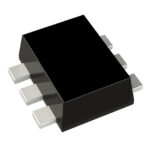 DMP68D1LV-13

The activity of extra discounts on wholesale prices is in full swing…
Please fill in your contact information and we will send you the latest wholesale price list.





