ChipApex | Global Electronic Components Supplier
SEARCH
Search Product
Search Post
— IC芯片 | 连接器 | 传感器 | 被动器件 —
Search productSearch post
— IC芯片 | 连接器 | 传感器 | 被动器件 —
Consult the customer manager about the wholesale price.
consultation hotline:86-132-6715-2157
email:[email protected]
Contact the product manager for consultation. One-stop consultation is available.
Do you want a lower wholesale price? Please send us your inquiry and we will reply immediately.
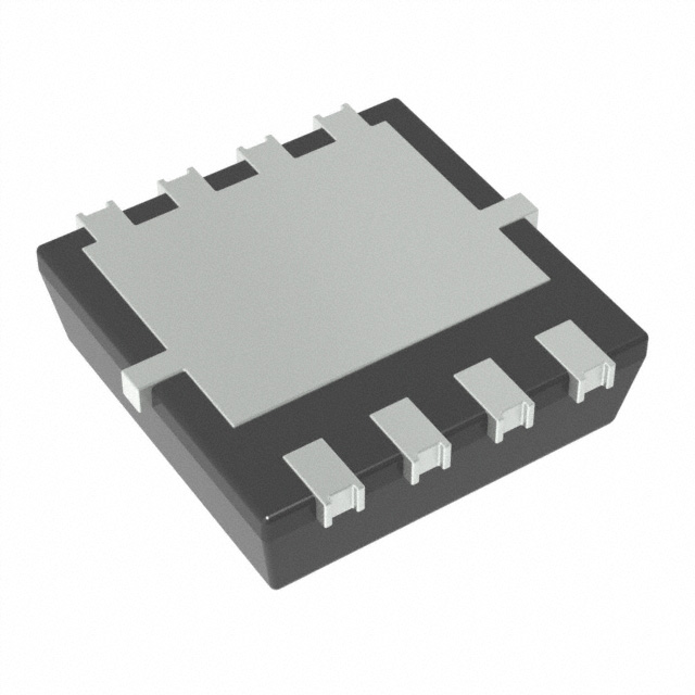
The DMPH4026SFVW-7 is a P-channel enhancement mode MOSFET from Diodes Incorporated, housed in a PowerDI3333-8 package. It features a drain-source voltage (BVDSS) of -40V and a maximum continuous drain current (ID) of -52A at TC = +25°C. The device offers a low on-state resistance (RDS(ON)) of 25mΩ at VGS = -10V and 45mΩ at VGS = -4.5V. It supports an operating temperature range from -55°C to +175°C and includes 100% UIS testing.
Verify the specific ordering suffix when purchasing. The '-7' suffix indicates a tape and reel packing quantity of 2000 units. Confirm that the required component matches this packaging format rather than the '-13' variant, which contains 3000 units per reel. Ensure the design accommodates the PowerDI3333-8 footprint and thermal requirements specified in the datasheet.
Select this component for applications requiring robust performance in elevated temperature conditions up to +175°C. The small form factor allows for higher density designs compared to traditional SO-8 packages. Evaluate the thermal resistance characteristics based on the specific PCB copper layout and mounting conditions to ensure adequate heat dissipation for the intended load currents.
This part belongs to Diodes Incorporated's new generation of MOSFETs designed to minimize on-state resistance while maintaining superior switching performance. It utilizes silicon technology within a molded plastic PowerDI® 3333-8 package. The device is manufactured with matte tin annealed terminals over a copper leadframe, ensuring solderability per MIL-STD-208 standards.
An automotive-compliant version of this component is available under the separate part number DMPH4026SFVWQ. Verify if AEC-Q101 qualification is required for the target application before selecting this standard industrial grade part or its automotive counterpart.
The maximum continuous drain current is -52A at a case temperature of +25°C and -38A at a case temperature of +100°C.
Yes, the datasheet specifies that 100% Unclamped Inductive Switch (UIS) testing is performed during production.
The gate threshold voltage (VGS(TH)) ranges from a minimum of -0.8V to a maximum of -1.8V, measured at VDS = VGS and ID = -250μA.
 DMPH4026SFVW-7
The activity of extra discounts on wholesale prices is in full swing…
Please fill in your contact information and we will send you the latest wholesale price list.