ChipApex | Global Electronic Components Supplier
SEARCH
Search Product
Search Post
— IC芯片 | 连接器 | 传感器 | 被动器件 —
Search productSearch post
— IC芯片 | 连接器 | 传感器 | 被动器件 —
Consult the customer manager about the wholesale price.
consultation hotline:86-132-6715-2157
email:[email protected]
Contact the product manager for consultation. One-stop consultation is available.
Do you want a lower wholesale price? Please send us your inquiry and we will reply immediately.
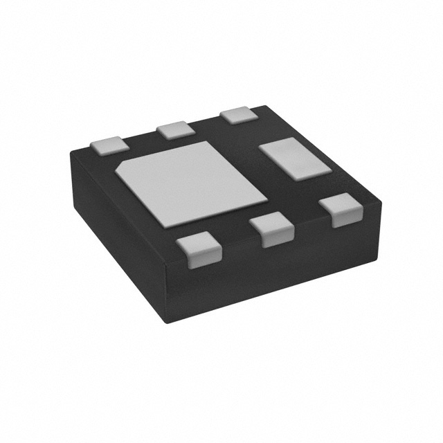
The DMT12H060LFDF-7 is a 115V N-channel enhancement mode MOSFET manufactured by Diodes Incorporated. It features a U-DFN2020-6 package with a 0.6mm profile and a 4mm² PCB footprint. The device provides a maximum drain-source breakdown voltage (BVDSS) of 115V and a continuous drain current (ID) of 4.4A at +25°C. Static drain-source on-resistance (RDS(ON)) is specified as 65mΩ max at VGS = 4.5V and 70mΩ max at VGS = 2.5V. Total gate charge (Qg) is typically 7.8nC. Operating temperature range spans from -55°C to +150°C.
Verify the specific ordering suffix when purchasing. The suffix '-7' indicates a standard reel packing quantity of 3,000 units in the U-DFN2020-6 package. The suffix '-13' corresponds to a larger reel containing 10,000 units. Confirm the required packaging format aligns with your manufacturing equipment capabilities before placing orders.
Select this component for designs requiring a 115V rating within a highly compact surface-mount form factor. The low thermal resistance and small footprint make it suitable for space-constrained portable electronics. Ensure the gate drive voltage meets the minimum requirements to achieve the lowest possible on-resistance values during operation.
This part belongs to Diodes Incorporated's new generation MOSFET lineup designed to balance low on-resistance with robust switching characteristics. It utilizes silicon technology housed in a specialized U-DFN2020-6 Type F package. The product line targets modern efficiency standards while maintaining compatibility with standard surface mount assembly processes.
Check datasheets for alternative parts offering similar 115V ratings and comparable RDS(ON) specifications. Verify pinout compatibility and physical dimensions if substituting directly into existing layouts. Ensure thermal management requirements remain met with any replacement component.
The single pulse avalanche energy rating is 21.6 mJ when tested with an inductance of 0.3mH.
For automotive applications requiring AEC-Q100/101/200 qualification or PPAP capability, customers must contact Diodes Incorporated directly as these require specific change control and manufacturing in IATF 16949 certified facilities.
The typical reverse recovery time is 24 ns when measured at a forward current of 3A and a di/dt of 300A/μs.
 DMT12H060LFDF-7
The activity of extra discounts on wholesale prices is in full swing…
Please fill in your contact information and we will send you the latest wholesale price list.