ChipApex | Global Electronic Components Supplier
SEARCH
Search Product
Search Post
— IC芯片 | 连接器 | 传感器 | 被动器件 —
Search productSearch post
— IC芯片 | 连接器 | 传感器 | 被动器件 —
Consult the customer manager about the wholesale price.
consultation hotline:86-132-6715-2157
email:[email protected]
Contact the product manager for consultation. One-stop consultation is available.
Do you want a lower wholesale price? Please send us your inquiry and we will reply immediately.
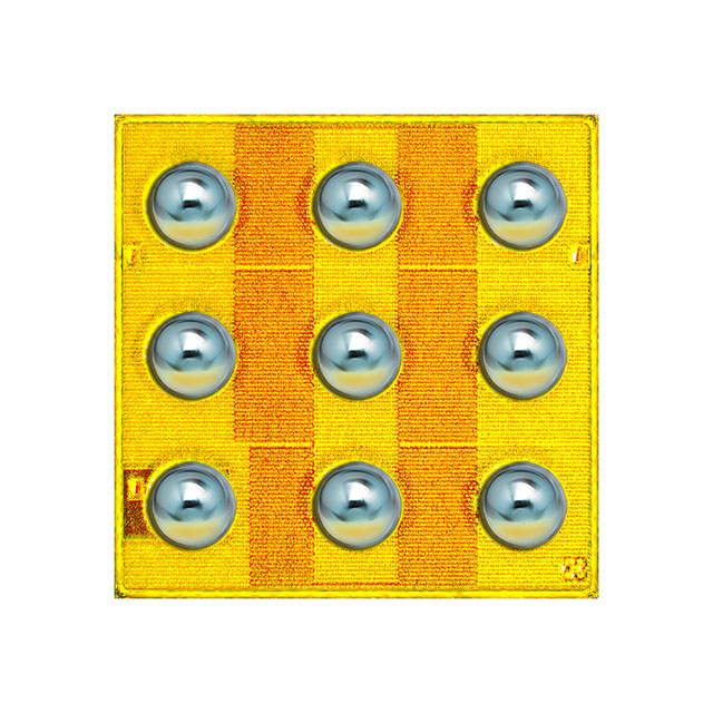
The EPC2052 is a GaN FET N-channel die with a drain-source voltage of 100 V and a continuous drain current of 8.2 A at Ta. It features a maximum gate-source voltage of +6 V/-4 V and a threshold voltage of 2.5 V @ 3 mA. The device has a maximum gate charge of 4.5 nC @ 5 V and an input capacitance of 575 pF @ 50 V. Its on-resistance is 13.5 mOhm @ 11 A, 5 V. Operating temperature ranges from -40°C to 150°C TJ.
Verify the specific package type, as this component is supplied as a die rather than a standard packaged device. Confirm compatibility with your substrate and assembly processes. Check for any recent product change notices regarding substrate suppliers or manufacturing locations. Ensure handling procedures account for the bare die nature of the component to prevent damage during installation.
Select this component when a 100 V rating and approximately 8.2 A continuous current are required in a minimal footprint. Consider its low gate charge and on-resistance for high-efficiency designs. Evaluate thermal management strategies suitable for direct die attachment. Compare against other devices in the 100 V Gen 5 family for specific performance trade-offs.
The EPC2052 belongs to the EPC 100 V Gen 5 family of enhancement-mode gallium nitride power transistors. These devices utilize advanced GaN technology to outperform traditional silicon MOSFETs in terms of speed and efficiency. The part is manufactured by Efficient Power Conversion (EPC) and is intended for integration into custom power modules or direct board-level implementations.
Consult official substitution guides for compatible parts within the EPC 100 V Gen 5 family. Verify pinout and electrical parameter equivalence before replacing existing silicon MOSFETs or other GaN dies. No direct public substitute part numbers are confirmed for this specific die configuration.
 EPC2052
The activity of extra discounts on wholesale prices is in full swing…
Please fill in your contact information and we will send you the latest wholesale price list.