ChipApex | Global Electronic Components Supplier

SEARCH
Search Product
Search Post
— IC芯片 | 连接器 | 传感器 | 被动器件 —
Search productSearch post
— IC芯片 | 连接器 | 传感器 | 被动器件 —
Consult the customer manager about the wholesale price.
consultation hotline:86-132-6715-2157
email:[email protected]
Contact the product manager for consultation. One-stop consultation is available.
Do you want a lower wholesale price? Please send us your inquiry and we will reply immediately.
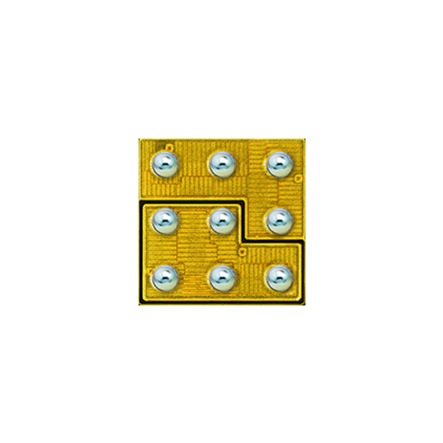
EPC2106ENGRT is listed in the FET, MOSFET Arrays range at ChipApex. The manufacturer field lists EPC. Its product description is MOSFET 2N-CH 100V 1.7A DIE. Review the specifications below when checking this part for your BOM.
The EPC2106 is an enhancement-mode Gallium Nitride (GaN) power transistor half-bridge. It features a 100 V drain-to-source voltage rating and a maximum on-resistance of 70 mΩ at 5 V gate drive. The device supports a continuous drain current of 1.7 A at 25°C and can handle pulsed currents up to 18 A. Total gate charge is typically 900 pC, with zero reverse recovery charge. Operating temperatures range from -40°C to +150°C junction temperature.
Verify the datasheet revision date against the manufacturer's official records before finalizing component selection. Confirm that the specific ordering suffix matches the required tape and reel dimensions for automated pick-and-place equipment. Ensure thermal management designs account for the specified junction-to-board resistance values.
Evaluate the 70 mΩ on-resistance against the target load current to determine conduction losses. Consider the 900 pC total gate charge when sizing the gate driver circuitry for switching speed requirements. Verify that the PCB land pattern strictly adheres to the recommended stencil drawing dimensions to ensure proper solder joint formation.
This component belongs to the eGaN FET family produced by Efficient Power Conversion Corporation. It utilizes lateral GaN technology to achieve high electron mobility and low temperature coefficients. The device is designed as a bare die intended for integration into custom printed circuit boards or hybrid modules.
No official substitute part numbers are documented in the provided datasheet. When selecting alternatives, match the 100 V breakdown voltage, half-bridge topology, and compatible package footprint. Verify that any replacement maintains similar gate charge characteristics to preserve existing driver performance.
The source-drain reverse recovery charge is 0.
The typical input capacitance is 95 pF at 50 V drain-to-source voltage.
The device is supplied only in passivated die form with solder bumps.
Explore related parts through FETs, MOSFETs, Transistors, Discrete Semiconductor Products, all product categories.
 EPC2106ENGRT

The activity of extra discounts on wholesale prices is in full swing…
Please fill in your contact information and we will send you the latest wholesale price list.