 ChipApex | Global Electronic Components Supplier
SEARCH
Search Product
Search Post
— IC芯片 | 连接器 | 传感器 | 被动器件 —
Search productSearch post
— IC芯片 | 连接器 | 传感器 | 被动器件 —
Consult the customer manager about the wholesale price.
consultation hotline:86-132-6715-2157
email:[email protected]
Contact the product manager for consultation. One-stop consultation is available.
Do you want a lower wholesale price? Please send us your inquiry and we will reply immediately.
The FCB099N65S3 is an N-channel power MOSFET from the SUPERFET III family, utilizing charge balance super-junction technology. It features a 650 V drain-source voltage rating and a maximum on-resistance of 99 mΩ at 10 V gate drive. The device supports a continuous drain current of 30 A at 25°C case temperature and handles pulsed currents up to 75 A. Key electrical parameters include a typical total gate charge of 61 nC and a typical effective output capacitance of 544 pF. It is housed in a D2PAK package.
Verify the specific ordering suffix and marking details against the manufacturer's official documentation before procurement. Confirm that the component meets all required environmental compliance standards, such as RoHS and lead-free specifications, for your intended application. Ensure thermal management designs align with the provided junction-to-case thermal resistance values.
Select this component for high-voltage applications requiring efficient power conversion with minimized EMI. Consider the 650 V breakdown voltage and low gate charge characteristics when designing for telecom or industrial environments. Evaluate the thermal dissipation requirements based on the specified power dissipation and derating curves to ensure reliable operation under expected load conditions.
This part belongs to the SUPERFET III series by onsemi, designed for high-voltage super-junction MOSFET applications. The series emphasizes low on-resistance and reduced gate charge to enhance overall system efficiency. It represents an evolution in power semiconductor technology aimed at simplifying design implementation while maintaining robust performance in demanding power supply architectures.
Consult official substitution guides for verified alternatives within the SUPERFET III family. Ensure any replacement matches the 650 V rating, D2PAK package dimensions, and electrical characteristics such as RDS(on) and Qg. Verify compatibility with existing thermal and PCB layout constraints before integration.
The absolute maximum drain-source voltage (VDSS) is rated at 650 V.
Yes, the datasheet specifies that these devices are 100% avalanche tested to ensure reliability under extreme conditions.
The component is available in a D2PAK package, also referred to as TO-263, with the case designation CASE 418AJ.
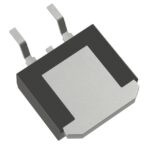 FCB099N65S3
The activity of extra discounts on wholesale prices is in full swing…
Please fill in your contact information and we will send you the latest wholesale price list.





