 ChipApex | Global Electronic Components Supplier
SEARCH
Search Product
Search Post
— IC芯片 | 连接器 | 传感器 | 被动器件 —
Search productSearch post
— IC芯片 | 连接器 | 传感器 | 被动器件 —
Consult the customer manager about the wholesale price.
consultation hotline:86-132-6715-2157
email:[email protected]
Contact the product manager for consultation. One-stop consultation is available.
Do you want a lower wholesale price? Please send us your inquiry and we will reply immediately.
The FCD260N65S3 is an N-channel enhancement mode MOSFET from onsemi's SUPERFET III series, utilizing super-junction charge balance technology. It features a 650V drain-source voltage rating and a maximum on-resistance of 260mΩ. The device supports a continuous drain current of 12A at case temperature and handles a pulsed current of 48A. Key electrical parameters include a gate threshold voltage of 2.5V, total gate charge of 37nC, and input capacitance of 1900pF. It operates within a junction temperature range of -55°C to +150°C and offers a power dissipation of 90W in the TO-252AA package.
Verify the specific suffix against the official datasheet to confirm pinout and thermal characteristics. Ensure the procurement channel provides valid traceability documentation. Confirm RoHS compliance status matches project requirements. Validate that the TO-252AA package dimensions align with the PCB footprint design specifications before finalizing orders.
Select this component when a compact surface-mount solution is required for high-voltage applications. The 260mΩ resistance balances cost and performance for moderate current levels. Consider the TO-252AA package for automated assembly processes. Evaluate thermal management needs based on the 90W dissipation rating under specified case temperatures.
This part belongs to the SUPERFET III family, representing onsemi's advanced super-junction MOSFET technology. It succeeds earlier SJ generations by offering improved figure-of-merit values through reduced gate charge and output capacitance. The series targets efficiency improvements in modern power supply designs requiring high voltage blocking capabilities.
Direct replacements must match the 650V rating, TO-252AA package, and similar Rds(on) and Qg values. Verify pin compatibility and thermal resistance parameters. Cross-reference with other SUPERFET III variants or equivalent super-junction devices from other manufacturers ensuring identical mounting and electrical constraints.
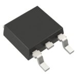 FCD260N65S3
The activity of extra discounts on wholesale prices is in full swing…
Please fill in your contact information and we will send you the latest wholesale price list.





